Conduction in Solids:
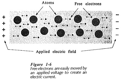
Conduction in Solids or any given material occurs when an applied voltage causes electrons within the material to move in a desired direction. This may be due to one or both of two processes; Electron Motion and Hole Transfer. In electron motion, free electrons in the Conduction band are moved under the influence of the applied electric field, thus creating an electric current, (see Fig 1-6). Since electrons have a negative charge, they are repelled from the negative terminal of the applied voltage and attracted toward the positive terminal. Hole transfer involves electrons which are still attached to atoms, (those in the valence band).
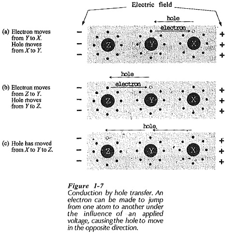
If some of the electron positions in the valence shell of an atom are not occupied by electrons, there are holes where electrons could exist. When sufficient energy is applied in Conduction in Solids, an electron may be made to jump from one atom to a hole in another atom. When it jumps, the electron leaves a hole behind it, and thus the hole has moved in a direction opposite to that of the electron.
Figure 1-7 illustrates a situation where there are no free electrons. However, those electrons in orbit around atoms experience a force of attraction to the positive terminal of the applied voltage, and repulsion from the negative terminal. This force can cause an electron to jump from one atom to another, moving toward the positive terminal.
Figure 1-7(a) shows an electron jumping from atom Y to atom X (toward the positive terminal of the applied voltage). When this occurs, the hole in the valence shell of atom X is filled, and a hole is left in the valence shell of atom Y, (Fig. 1-7(b)]. If an electron now jumps from atom Z to fill the hole in Y, a hole is left in the valence shell of Z, [Fig. 1-7(c)]. Thus, the hole has moved from atom X to atom Y to atom Z. So, a flow of current (electron motion) has occurred, and this may be said to be due to hole movement, or hole transfer.
Holes may be thought of as positively charged particles, and as such, they move through an electric field in a direction opposite to that of electrons. (Positive particles are attracted toward the negative terminal of an applied voltage.) In the circumstance illustrated in Fig. 1-7 where there are few free electrons, it is more convenient to think in terms of hole movement rather than in terms of electrons jumping from atom to atom.
Since the flow of electric current is constituted by the movement of electrons and holes, electrons and holes are referred to as charge carriers. Each time a hole moves, an electron must be supplied with sufficient energy, to enable it to escape from its atom. Free electrons require less application of energy than holes to move them, because they are already disconnected from their atoms. For this reason, electrons have greater mobility than holes.
Direction of Conventional Current and Electron Flow:
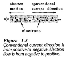
In the early days of electrical experimentation in Conduction in Solids was believed that a positive charge represented an increased amount of electricity, and that a negative charge was a reduced quantity. Thus, it was assumed that current flowed from positive to negative. This is a convention that remains in use today even though current is now known to be a movement of electrons from negative to positive, (see Fig. 1-8).
- Current flow from positive to negative is referred to as the conventional current direction.
- Electron flow from negative to positive is known as the direction of electron flow.
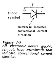
It is important to understand both electron flow and conventional current direction in Conduction in Solids. The operation of electronic devices is explained in terms of electron movement. However, every graphic symbol used to represent an electronic device has an arrowhead which indicates conventional current direction, (see the diode symbol in Fig. 1-9). Consequently, electronic circuits are most easily explained by using current flow from positive to negative.


