Tunnel Diode Equivalent Circuit:
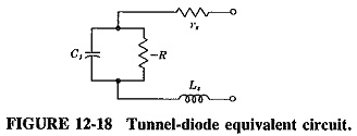
The Tunnel Diode Equivalent Circuit, when biased in the negative-resistance region, is shown in Figure 12-18. At all except the highest frequencies, the series resistance and inductance can be ignored. The resulting diode equivalent circuit is thus reduced to the parallel combination of the junction capacitance Cj and the negative resistance – R. Typical values of the circuit components of Figure 12-18 are rs = 6 Ω, Ls = 0.1 nH, Cj = 0.6 pF and R = -75 Ω.
The tunnel diode was the first, and for several years the only, solid-state device which merely required the application of a small dc voltage for negative resistance to manifest itself. However, after the initial exclamations of joy at the remarkable invention died down, tunnel diode oscillators were found to be unstable in their frequency of operation and were all but discarded. The reasons for the instability have subsequently been found and cured, and so Tunnel Diode Equivalent Circuit are again in use, but now mainly for amplifiers.
The junction capacitance of the Tunnel Diode Equivalent Circuit is highly dependent on the bias voltage and temperature. Connecting a tuned circuit directly across it will undoubtedly yield an unstable oscillator, particularly since the effective Q of the circuit is relatively low. However, if a high-Q cavity is loosely coupled to the diode, a highly stable Oscillator is obtained, with a relative independence of temperature, bias voltage or diode parameter variation.
Description of Behavior:
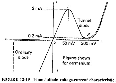
The tunnel diode is a semiconductor p-n junction diode. It differs from the usual rectifier-type diodes in that the semiconductor materials are very heavily doped, perhaps as much as 1000 times more than in ordinary diodes. This heavy doping results in a junction which has a depletion layer that (with a typical thickness of 0.01 μm) is so thin as to prevent tunneling to occur. In addition, the thinness of the junction allows microwave operation of the diode because it considerably shortens the time taken by the carriers to cross the junction. A current-voltage characteristic for a typical germanium tunnel diode is shown in Figure 12-19. It is seen that at first forward current rises sharply as voltage is applied, where it would have risen slowly for an ordinary diode (whose characteristic is shown for comparison). Also, reverse current is much larger for comparable back bias than in other diodes, owing to the thinness of the junction.
The interesting portion of the characteristic begins at the point A on the curve of Figure 12-19; this is the voltage peak. As the forward bias is increased past this point, the forward current drops and continues to drop until point B is reached; this is the valley voltage. At B the current starts to increase once again and does so very rapidly as bias is increased further. From this point the characteristic resembles that of an ordinary diode. Apart from the voltage peak and valley, the other two parameters normally used to specify the diode behavior are the peak current and the peak-to-valley current ratio, which here are 2 mA and 10, respectively, as shown.
The diode voltage-current characteristic illustrates two important properties of the Tunnel Diode Equivalent Circuit. First it shows that the diode exhibits dynamic negative resistance between A and B and is therefore useful for oscillator (and amplifier) applications. Second since this negative resistance occurs when both the applied voltage and the resulting current are low, the Tunnel Diode Equivalent Circuit is a relatively low-power device. A quick calculation shows that in order to stay within the negative-resistance region, the voltage variation must be restricted to 300 – 50 = 250 mV (peak-to-peak) = 88.4 mV rms, whereas the current range is similarly 1.8 mA (peak-to-peak) = 0.63 mA. The load power is very roughly 88.4 x 0.635 = 56 μW. Other factors have been neglected, but the figure is of the right order.
Diode Theory:
Unless energy is imparted to electrons from some external source, the energy possessed by the electrons on the n side of the junction is insufficient to permit them to climb over the junction barrier to reach the p side. Quantum mechanics shows that there is a small but finite probability that an electron which has insufficient energy to climb the barrier can, nevertheless, find itself on the other side of it if this barrier is thin enough, without any loss of energy on the part of the electron. This is the tunneling phenomenon which is responsible for the behavior of the diode over the region of interest.
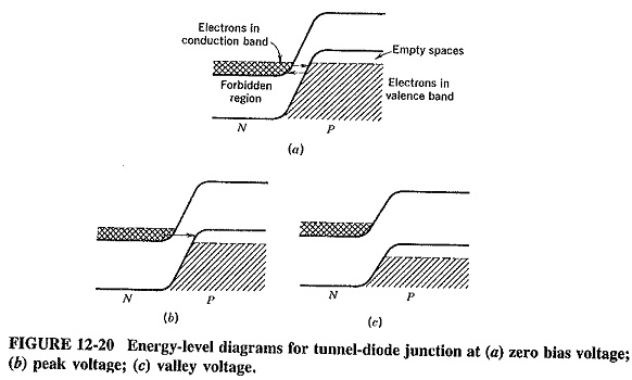
Figure 12-20 shows energy-level diagrams for the Tunnel Diode Equivalent Circuit for three interesting bias levels. The cross-hatched regions represent energy states in the conduction band occupied by electrons, whereas the shaded areas show the energy states occupied by electrons in the valence bands. The levels to which energy states are occupied by electrons on either side of the junction are shown by dotted lines. When the bias voltage is zero, these lines are at the same height. Electrons can now tunnel from one side of the junction to the other because of its thinness, but the tunneling currents in the two directions are the same. No effective overall current flows. This is shown in Figure 12-20a.
When a small forward bias is applied to the junction, the energy level of the p side is lowered (as compared with the n side). As shown in Figure I2-20b, electrons are able to tunnel through from the n side. This is possible because the electrons in the conduction band there find themselves opposite vacant states on the p side. Tunneling in the other direction is not possible, because the valence-band electrons on the p side are now opposite the forbidden energy gap on the n side. This gap, shown here at its maximum, represents the peak of the diode characteristic.
When the forward bias is raised beyond this point, tunneling will decrease, as may be seen with the aid of Figure 12-20c. The energy level on the p side is now depressed further, with the result that fewer n-side free electrons are opposite unoccupied p-side energy levels. As the bias is raised, forward current drops; this corresponds to the negative-resistance region of the diode characteristic. As Figure 12-20c shows, a forward bias is reached at which there are no conduction-band electrons opposite valence-band vacant states, and tunneling stops altogether. The point at which this happens is the valley of Figure 12-19, to which the energy-level diagram of Figure 12-20c corresponds. When forward voltage is increased even further, “normal” forward current flows and increases, as with ordinary rectifier diodes.
It is thus seen that the curious phenomenon in tunnel diodes is not only the negative-resistance region but also the forward current peak that precedes it. As a result of tunneling across the narrow junction, forward current flows initially in much greater quantities than in a rectifier diode. As the forward bias is raised, tunneling becomes more difficult, the tunneling current is reduced and the negative-resistance region results. As the increase in forward voltage continues, tunneling stops completely, and the normal operation takes over. The valley is the point at which this “return to normalcy” begins.
Materials and Construction:
Although Tunnel Diode Equivalent Circuit could be made from any semiconductor material, initially germanium and then gallium antimonide and gallium arsenide have been preferred in practice. All have small forbidden energy gaps and high ion mobilities, which are characteristics leading to good high-frequency or high-speed operation. These materials are preferable to silicon and other semiconductors in this regard.
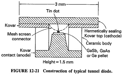
As the cross section of Figure 12-21 shows, the construction of a tunnel diode is remarkably simple. This is yet another advantage of the device, particularly since the fabrication is also simple. A very small tin dot, about 50 μm in diameter, is soldered or alloyed to a heavily doped pellet (about 0.5 mm square) of n-type Ge, GaSb or GaAs. The pellet is then soldered to a Kovar pedestal, used for heat dissipation, which forms the anode contact. The cathode contact is also Kovar, being connected to the tin dot via a mesh screen used to reduce inductance. The diode has a ceramic body and a hermetically sealing lid on top. Note the tiny dimensions of the pill package.


