Pin Diode Construction:
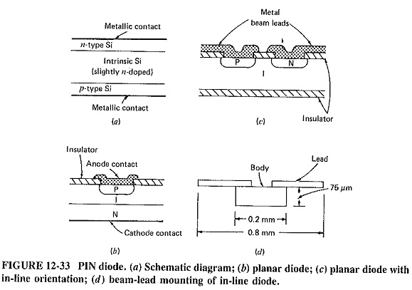
The Pin Diode Construction consists of a narrow layer of p-type semiconductor separated from an equally narrow layer of n-type material by a somewhat thicker region of intrinsic material. The intrinsic layer is a lightly doped n-type semiconductor. The name of the diode is derived from the construction (p-intrinsic-n). Although gallium arsenide is used in the construction of PIN diodes, silicon tends to be the main material. The reasons for this are easier fabrication, higher powers handled and higher resistivity of intrinsic region. The PIN diode is used for microwave power switching, limiting and modulation. It was first proposed by R. N. Hall in 1952, and its potential as a microwave switch was first recognized by Uhlir in 1958.
Construction:
The construction of the PIN diode is shown in Figure 12-33. The advantage of the planar construction is the lower series resistance while conducting. Encapsulation for such a chip takes any of the forms already shown for other microwave diodes.
The in-line construction has a number of advantages, including reduced diode shunt capacitance. Also, as shown in Figure 12-33c and d, it lends itself ideally to beam-lead encapsulation, thus inter-working excellently with stripline circuits. This construction is often preferred in practice, except perhaps for the highest powers. When fairly large dissipation are involved, the planar construction is better adapted to mounting on a heat sink.
Operation:
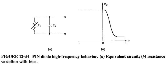
The PIN diode acts as a more or less ordinary diode at frequencies up to about 100 MHz. However, above this frequency it ceases to be a rectifier, because of the carrier storage in, and the transit time across, the intrinsic region. At microwave frequencies the diode acts as a variable resistance, with a simplified equivalent circuit as in Figure 12-34a and a resistance-voltage characteristic as in Figure 12-34b.
When the bias is varied on a PIN diode, its microwave resistance changes from a typical value of 5 to 10 kΩ under negative bias to the vicinity of 1 to 10 Ω when the bias is positive. Thus, if the diode is mounted across a 50-Ω coaxial line, it will not significantly load the line when it is back-biased, so that power flow will be unaffected. When the diode is forward-biased, however, its resistance becomes very low, so that most of the power is reflected and hardly any is transmitted.
The diode is acting as a switch. In a similar fashion, it may be used as a (pulse) modulator. Several diodes may be used in series or in parallel in a waveguide or coaxial line, to increase the power handled or to reduce the transmitted power in the OFF condition.
Performance and Applications:
Diodes are available with resistive cutoff frequencies up to about 700 GHz. As for varactor diodes, the operating frequencies do not exceed one-tenth of the above figure. At least one instance of operation at 150 GHz, with specially constructed diodes, has been reported. Individual diodes may handle up to about 200 kW peak (or 200 W average), although typical levels are one magnitude lower.
Several diodes may be combined to handle as much as 1 MW peak. Actual switching times vary from approximately 40 ns for high-power limiters to as little as 1 ns at lower powers.

