Biasing Bipolar Op Amp Circuit:
Biasing Bipolar Op Amp Circuit – Like other electronic devices, operational amplifiers must be correctly biased if they are to function properly. As already discussed, the inputs of an operational amplifier are the base terminals of the transistors in a differential amplifier. Base currents must flow into these terminals for the transistors to operate. Consequently, the input terminals must be directly connected to suitable dc bias voltage sources.
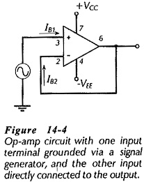
The most appropriate dc bias voltage level for Biasing Bipolar Op Amp Circuit inputs is approximately halfway between the + and – supply voltages. One of the two input terminals is usually connected in some way to the op-amp output to facilitate negative feedback. Where a +/- supply is used, the other input might be biased directly to ground via a signal source [see Fig. 14-4]. Base current IB1 flows into the op-amp noninverting input via the signal source, while IB2 flows from the output into the inverting input, as illustrated.
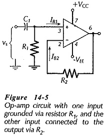
Figure 14-5 shows a situation in which one input is connected via resistor R1 to ground, and the other is connected via R2 to the op-amp output. Once again base current for the input stage transistors flows into both input terminals. R1 and R2 should have equal resistance values, so that voltage drops IB1R1 and IB2R2 are approximately equal. Any difference in these two voltage drops appears as an op-amp dc input voltage which may be amplified to produce a dc offset at the output.
If very small resistance values are selected for R1 and R2 in the circuit in Fig. 14-5, then a very small input resistance (R1) would be offered to a capacitor-coupled signal source, [see Fig. 14-5]. On the other hand, if R1 and R2 are very large, the voltage drops IB1R1 and IB2R2 might be ridiculously large. An acceptable maximum voltage drop across these resistors must be very much smaller than the typical VBE level for a forward-biased base-emitter junction.
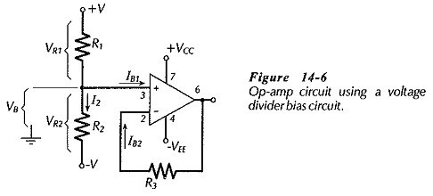
Figure 14-6 shows a voltage divider (R1 and R2) providing an input terminal bias level from the the supply voltages. The voltage divider current I2 should be selected to be very much larger than the input bias current. This is to ensure that IB has a negligible is selected as,
Then R1 and R2 are simply calculated as, VR1/I2 and VR2/I2 respectively.
Resistor R3 in Fig. 14-6 should be selected approximately equal to R1||R2 to minimize any difference between IB1(R1||R2) and IB1R3 that could behave as a dc input voltage.
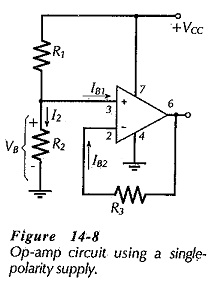
A single-polarity supply voltage can be used with an Biasing Bipolar Op Amp Circuit. For example, a 741 could use a +30 V (as illustrated in Fig. 14-8) instead of a ±15 V supply. Resistors R1 and R2 are normally selected to set VB = VCC/2.
The resultant output offset, can be reduced or eliminated in the circuit shown in Fig. 14-6 by making one of the resistors adjustable. Similarly, if R3 in Fig. 14-8 is a variable resistor, it could be adjusted to reduce the op-amp output offset voltage. The process is termed voltage offset nulling.
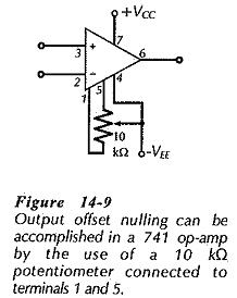
Figure 14-9 shows another method of voltage offset nulling with a 741 op-amp. A 10 kΩ potentiometer is connected to the differential amplifier input stage via terminals 1 and 5, as illustrated. With the moving contact connected to -VEE, the potentiometer can be adjusted to null the output offset voltage.
Biasing BIFET Op-amps:
The input bias current for a BIFET op-amp is typically 50 pA, which is very much smaller that that for a Bioplar op-amp. So, the bias resistor selection method already discussed would produce very high resistor values. This is undesirable because electric charges can accumulate at the FET gates, and thus make the bias levels unstable. Also, stray capacitance becomes more effective with high value bias resistors, possibly resulting in unwanted circuit oscillations. To combat these effects, the largest resistor in a BIFET op-amp bias circuit should normally not exceed 1 MΩ.
