Direct Coupled Inverting Amplifier:
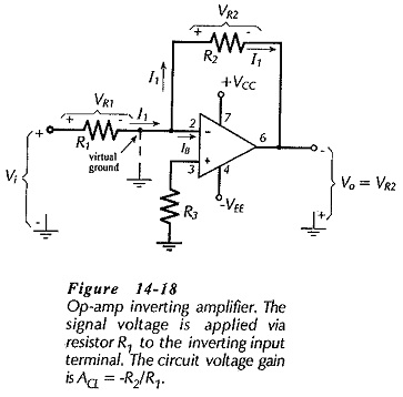
The circuit in Fig. 14-18 is termed an Direct Coupled Inverting Amplifier because, with Vi applied via R1 to the inverting input terminal, the output goes negative when the input goes positive, and vice versa. Note that the noninverting input terminal is grounded via resistor R3. With the noninverting terminal grounded, the voltage at the op-amp inverting input terminal remains close to ground. Any increase or decrease in the (very small) difference voltage between the two input terminals is amplified by the op-amp open-loop gain and fed back via R2 and R1 to correct the change. Because the inverting input terminal is not grounded but remains close to ground, the inverting input terminal in this application is termed a virtual ground or virtual earth.
The circuit input current in Fig. 14-18 can be calculated as,
The input voltage is applied to one end of R1, and the other end of R1 is at ground level. Consequently,
I1 is always selected to be very much larger than the op-amp input bias current (IB). Consequently, virtually all of I1 flows through resistor R2, (see Fig.14-18), and the voltage drop across R2 is,
The left side of R2 is connected to the op-amp inverting input terminal, which, as discussed, is always at ground level. This means that the right side of R2 (the output terminal) is VR2 below ground. So,
From Eq. 14-10, Vi = I1R1
So, the circuit voltage gain is,
If the input of the inverting amplifier is grounded, the circuit is seen to be exactly the same as noninverting amplifier with R3 as the input resistor and zero input voltage. Thus, negative feedback occurs (as in a noninverting amplifier) to maintain the op-amp inverting input terminal at the same voltage level as the noninverting input terminal.
The output impedance of an inverting amplifier is calculated in exactly the same way as for a noninverting amplifier, (using Eq. 13-6). Like the case of the noninverting amplifier, the output impedance is very low for an inverting amplifier.
The input impedance of an inverting amplifier is easily determined by recalling that the right side of R1 (in Fig. 14-18) is always at ground level, and that the signal is applied to the left side of R1. Therefore,
Design of an inverting amplifier is very simple. Voltage divider current I1 is selected very much larger than the op-amp input bias current. Resistors R1 and R2 are calculated from Eqs. 14-10 and 14-11, or 14-12, and R3 is selected approximately equal to R1||R2.
Capacitor-Coupled Inverting Amplifier:
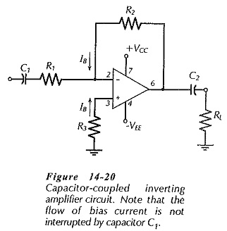
A capacitor-coupled inverting amplifier circuit is shown in Fig. 14-20. In this case, the bias current to the op-amp inverting input terminal flows (from the output) via resistor R2, so that the input coupling capacitor does not interrupt the input bias current. A voltage drop IBR2 is produced at the inverting input by the bias current flow, and this must be equalized by the IBR3 voltage drop at the noninverting input. ‘Therefore, for the capacitor-coupled noninverting circuit,
Apart from the selection of R3, the circuit is designed exactly as the Direct Coupled Inverting Amplifier, and the capacitor values are calculated in the same way as for a capacitor-coupled noninverting amplifier.


