Improving Regulator Performance:
Error Amplifier Gain – The performance of a regulator is dependent on the voltage gain of the error amplifier. A higher gain amplifier gives better line and load regulation. So, anything that improves the amplifier voltage gain will improve the regulator performance. Two possibilities to increase Av are: using as transistor with a high hFE value for Q2, and using the highest possible resistance value for R1.
Output Voltage Adjustment:
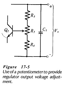
Regulator circuits such as the one designed are unlikely to have Vo exactly as specified. This is because of component tolerances, as well as, perhaps, not finding standard values close to the calculated values. Hence, some form of adjustment is required to enable the output voltage to be set to the desired level. In Fig. 17-5 the potentiometer (R5) connected between resistors R3 and R4 provides output adjustment. The maximum output voltage level is produced when the potentiometer moving contact is at the bottom of R5:
Minimum Vo occurs when the moving contact is at the top of R5:
High Output Current Circuit:
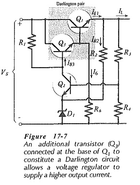
For the circuit in Fig. 17-6 to function correctly, the collector current of Q2 must be larger than the maximum base current flowing into Q1. In regulators that supply a large output current, IB1 can be too large for IC2 to control. In this case, an additional transistor (Q3) should be connected at the base of Q1 to form a Darlington Circuit (or Darlington Pair), as in Fig. 17-7. Transistor Q1 is usually a high power BJT requiring a heat sink and Q3 is a low power device. The Q3 base current is,
The current gain for the Darlington is (hFE1 X hFE3), and the level of IB3 is low enough that IC2 may easily be made much greater than IB3. Note resistor R6 in Fig. 17-7, which is included to provide a suitable minimum Q3 operating current when IL is very low.
Darlington transistors consisting of a pair of (low-power and high-power) BJTs fabricated together and packaged as a single device are available, These are usually referred to as power Darlington. The 2N6039 is an npn power Darlington with an hFE specified as 750 minimum, 18 000 maximum. Resistor R6 in Fig. 17-7 is not required when a power Darlington is used.
Preregulation:
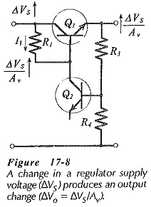
Refer to Fig. 17-8, which is a partially reproduction of Fig. 17-2. Note that resistor R1 is supplied from the regulator input, and consider what happens when, the supply voltage drops by 1 V. If IC2 does not change, the voltage across R1 remains constant, and the 1 V drop also occurs at the base of Q1 and at the output of the regulator. This does not happen, of course. Instead, IC2 changes to reduce the voltage across R1 and thus keep the output voltage close to its normal level. The change in IC2 is produced by a small change in the output voltage. If R1 is connected to a constant-voltage source instead of the input, the change in IC2 would not be required when VS changes, and consequently, the output voltage change would not occur.
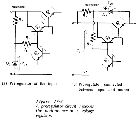
Now look at Fig. 17-9(a) where R1 is shown connected to another Zener diode voltage source (R7 and D2). This arrangement is called a preregulator. When VS changes, the change in VZ2 that occurs is negligible compared to ΔVS. Thus, virtually no change is required in IC2 and Vo. A preregulator substantially improves the line and the load regulation of a regulator circuit.
The minimum voltage drop across R1 should typically be 3 V. (Small values of R1 give low amplifier voltage gain.) Also, a minimum of perhaps 6 V is required across R7 to keep a reasonably constant current level through D2. The The voltage (VZ2) for D2 is usually a relatively high voltage for a Zener diode. It may be necessary to use two diodes in series to give the desired voltage.
Figure 17-9(b) shows another preregulator circuit that has R7 and D2 connected across transistor Q1. This gives an R1 supply voltage of V1 = (Vo + VZ2).
Constant Current Source:
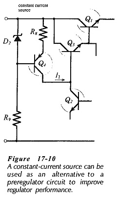
The constant-current source shown in Fig. 17-10 may be used in place of resistor R1 as an alternative to a preregulator circuit. This arrangement passes all the required current to Q3 base and Q2 collector, but behaves as a very high resistance (1/ hoe4) at the collector of transistor Q2. Consequently, it increases the error amplifier voltage gain and results in a substantial improvement in the regulator performance. To design the constant current source VCE4 should typically be a minimum of 3 V. The various voltage drops and current levels are then easily determined for component selection.
Differential Amplifier:
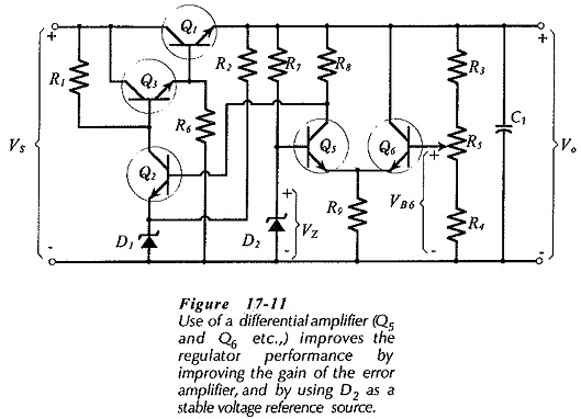
Figure 17-11 shows a regulator that uses a differential amplifier, or difference amplifier. In this circuit, Zener diode D2 is the voltage reference source, and D1 is used only to provide an appropriate voltage level at the emitter of transistor Q2. Vo is divided to provide VB6, and VB6 is compared to VZ2. Any difference in these two voltages is amplified by Q5, Q6, Q2, and the associated components, and then applied to the base of Q3 to change the output in the required direction.
The performance of the regulator is improved by the increased voltage gain of the error amplifier. However, the performance is also improved in another way. In the regulator circuit in Figs. 17-2 and 17-7, when IC1 changes, the current through D1 is also changed, (IZ1 = IR2 + IE2). This causes the Zener voltage to change by a small amount, and this change in VZ1 produces a change in output voltage. In the circuit in Fig. 17-11, the current through the reference diode (D2) remains substantially constant because it is supplied from the regulator output. Therefore, there is no change in output voltage due to a change in the reference voltage.
