Capacitor Coupled Class AB Output Stage:
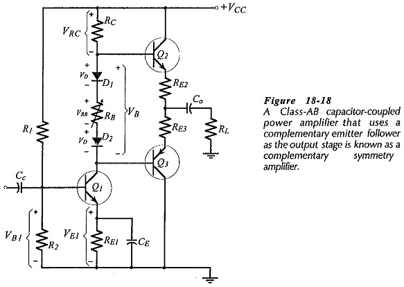
The basic circuit of a Class-AB amplifier using a complementary emitter follower output stage and a Capacitor Coupled Class AB Output Stage load is shown in Fig. 18-18. The circuit is termed a complementary symmetry amplifier. Transistor Q1 and resistors R1, R2, RC, and RE1 comprise a common emitter amplifier stage that produces all of the circuit voltage gain. The output of Q1 is developed across RC and applied to the bases of Q2 and Q3. Capacitor Co ac couples RL, and dc isolates RL to keep it from affecting the circuit bias conditions.
The total voltage drop (VB) across diodes D1 and D2 and resistor RB forward biases the base-emitter junctions of Q2 and Q3 to avoid cross-over distortion. Emitter resistors RE2 and RE3 help limit the quiescent current through Q2 and Q3. Adjustment of the bias voltage (VB) is provided by variable resistor RB. The diodes have voltage drops (VD) that approximately match the, output transistor VBE levels. Also, VD does not change significantly when the diode current changes, so, the diodes behave like bypassed resistors. The diodes and output transistors can be thermally-coupled by mounting D1 and Q2 on a single heat sink, and D2 and Q3 on a single heat sink. In this case, VD follows the VBE level changes with temperature, thus stabilizing the transistor bias conditions over a wide temperature range. The junction of RE2 and RE3 must be biased to VCC/2, so that the output voltage to Co can swing by equal amounts in positive- and negative-going directions.
Class-AB Capacitor-Coupled Amplifier Design:
Design of the type of circuit shown in Fig. 18-18 is largely a matter of selecting appropriate resistor voltage drops and current levels, and then applying Ohm’s law to calculate the resistor values. The peak output voltage (VP) and peak output current (IP) can be determined from earlier Equations, respectively. Those equations were developed for the power delivered to a transformer primary, but they apply equally to power delivered to any load resistor.
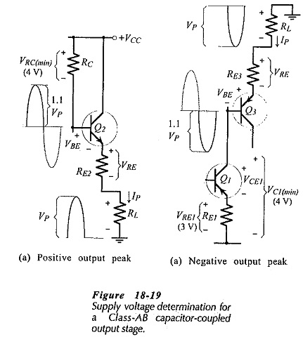
The voltage drops across RE2 and RE3 when the peak output current is flowing are typically selected as 5% to 10% of the peak output voltage. This is illustrated in Fig. 18-19(a) and (b) where the output capacitor is represented as an ac short-circuit. So,
It should be remembered that RE2 and RE3 are included to help stabilize the transistor quiescent currents at a level that eliminates cross-over distortion in the output waveform. For the type of amplifier circuit in Fig. 18-18, without overall negative feedback, it is best to select the emitter resistors as large as possible. Smaller emitter resistors can be used in circuits with dc and ac negative feedback.
When the output is at its negative-going peak, VCE1 should be 1 V minimum, to ensure that Q1 does not go into saturation. Also, VE1 should typically be 3 V. So, the minimum level of VC1 is typically 4 V, [Fig. 18-19(b)]. Similarly, when the output is at its positive-going peak, there must be an appropriate minimum voltage drop across resistor RC, [Fig. 18-19(a)]. It is not acceptable to set a 1 V minimum for VRC, because the current through RC would be too Small for the required peak base current to Q2. So, it is best to select,
The minimum current through (IRC(min)) should typically be selected 1 mA larger than the peak base current for the output transistors. RC is calculated from VRC(min) and IRC(min).
Referring to Fig. 18-19(a), the supply required to produce the positive output peak voltage is
Also, from Fig. 18-19(b), the negative output peak requires,
So, the total supply voltage is,
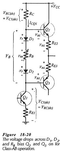
The voltage drop across the diodes and RB should just bias Q2 and Q3 on for Class-AB operation, (see Fig. 18-20). The current through RB is the Q1 quiescent current (ICQ1), and this is calculated from RC and the dc voltage drop across RC. VRC(dc) equals VC1(dc), and the sum of them equals (VCC – VB), (see Fig. 18-20). So,
The resistance of RB is now calculated from VRC(dc) and ICQ1. Resistors R1, R2, and RE1 are determined in the usual manner for an emitter current bias circuit.
The output transistors should be specified in terms of their maximum voltage, current, and power dissipation. The maximum VCE for Q2 and Q3 (in Fig. 18-18) is the total supply voltage (VCC). Maximum current for Q2 and Q3 is the peak load current plus the selected quiescent current (IQ23). This normally 1.1 Ip. Transistor power dissipation is calculated by determining the dc power delivered to the output stage from the power supply, and then subtracting the ac load power. The remainder is halved to find the power dissipated in each transistor. Equation 18-12 applies; PT = 0.5 (Pi – Po). Recall that the transistors must be operated within the safe operating area of the characteristics.
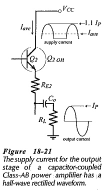
With a capacitor-coupled load, current is drawn from the power supply during the positive half-cycle of the output, but not during the negative half cycle. The capacitor acts as an energy reservoir to supply load current when the output is negative-going. Consequently, the supply current has a half-wave rectified waveform (see Fig. 18-21), and so,
The dc supply power to the output stage is,
As always, with the exception of the capacitor selected to set the circuit low 3 dB frequency (f1), each capacitor impedance is selected as one tenth of the impedance in series with the capacitor. Where there is no overall negative feedback, the capacitor with the lowest-value series-connected impedance is normally selected to set f1. For the circuit shown in Fig. 18-18, the impedance looking into the emitter of Q1 is hib1, and this is in series with CE. If hib1 is smaller than RL, then at f1;
Most power amplifiers typically have RL = 8 Ω or 16 Ω. So, the load-coupling capacitor normally sets the circuit low 3 dB frequency.


