n Stage Cascaded Amplifier:
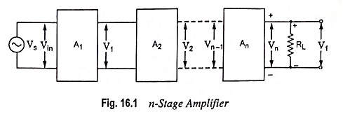
As already discussed, several amplifier stages are usually cascaded to increase the overall voltage gain of the amplifier. However, sometimes cascading is done to obtain the desired output and input impedance for specific applications. Block diagram of an n stage cascaded amplifier is given in Fig. 16.1. The first stage is driven by a voltage source Vs (or a current source Is). The output of first stage is fed to the input of the second stage, the output of second stage is supplied to the input of the third stage and so on. The output of the nth or last stage is fed to the load RL. Actual voltage available at the input of the first stage is Vin (Vin equals signal voltage Vs if source resistance Rs is negligible) and the voltage available at the output terminals of the last stage is Vout. Then the ratio Vout/Vin provides the voltage gain of the n-stage cascaded amplifier. Thus by designing properly a cascaded amplifier, a weak input signal Vin of just a few microvolts can be amplified giving output voltage Vout of several volts.
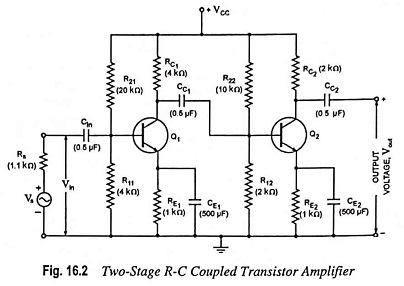
Here we take up R-C coupled amplifier, being the most popular amplifier employed for audio-frequency amplification. A typical two-stage R-C coupled amplifier using N-P-N transistors in common emitter configuration (the most suitable transistor configuration for cascading) is given in Fig. 16.2. Typical values of circuit components are given in the brackets.
The block diagram of a two stage R-C coupled transistor amplifier shown in Fig. 16.2 indicating the various voltages, currents and resistances involved is given in Fig. 16.3. The biasing arrangements and coupling capacitors have been omitted for sake of simplicity and clarity.
1. Voltage Gain: The overall voltage gain of the amplifier is given by the product of the voltage gains of the individual stages. This is proved as below :
Voltage gain of first stage,
where Av1 is the magnitude of the voltage gain of the first stage and θ1 is the phase angle between output and input voltages of this stage.
Similarly the voltage gain of nth stage,
Thus the overall voltage gain of the complete n-stage cascaded amplifier is given as
where Av is the magnitude of the voltage gain and θ is the phase angle between the output and input voltages of the amplifier.
Since
Hence
Thus it is concluded that the magnitude of the overall voltage gain equals the product of the magnitudes of the voltage gains of the individual stages and the resultant phase shift of the amplifier equals the sum of the phase shifts introduced by individual stages.
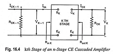
The voltage gain of kth stage (an intermediate stage) of an n-stage CE cascaded amplifier shown in Fig. 16.4 is given as
where RLK is the effective load at the collector of the kth stage.
The quantities in above equation (i.e. Aik, RLk and Rin k) are evaluated by starting with the last stage and proceeding backward. Thus for the nth stage, current gain Ain and input resistance Rin n are given as
where RLn is the effective load impedance of the final (i.e. nth) stage and equals Rcn.
For the (n – 1)th stage, effective load impedance Rin n-1 equals Rcn-1 || Rin n. So
Now the current gain Ai (n – ), of the last but one stage [i.e. (n – 1)th stage] is obtained using Eq. (16.11) by replacing RL n by RL n – 1. Similarly the input impedance Rin n – 1 of the (n – 1)th stage is determined from Eq. (16.12) by replacing Ain by Ai n – 1 and RL n by RL n – 1. Thus proceeding backward, base-to-collector current gains and input impedances of every stage including the first one can be determined. Then the voltage gain of each stage can be determined by using Eq. (16.10).
Overall voltage gain of the n-stage cascaded amplifier may then be calculated from Eq. (16.6).
2. Current Gain: Overall voltage gain of an n-stage cascaded amplifier can be obtained, without determining the voltage gain of individual stage, from the following equation
where Ai is the overall current gain of the n-stage cascaded amplifier and
where Icn ≡ In, the collector current of the nth stage.
Now let us obtain equations so as to calculate current gain Ai in terms of circuit parameters.
Since
where Ai1 is the base-to-collector current gain of the first stage and is equal to -Ici/Ibi while A′i2, A′i3 etc. are the collector-to-collector current gains of second, third etc. stages.
For kth stage, collector-to-collector current gain A′ik is given as
Similarly base-to-collector current gain of kth stage Aik is given as
Now from Fig. 16.4,
where Rin k is the input impedance of the kth stage.
Hence
Base-to-collector current gain Aik is determined by starting with the output stage and proceeding backward to the kth stage, as indicated in connection with Eqs. (16.11), (16.12) and (16.13). The collector-to-collector current gains are then determined by using Eq. (16.20) and the overall current gain of the n-stage amplifier is determined by using Eq. (16.16).
3. Input Impedance: The input impedance of the complete cascaded amplifier is determined, as discussed above, by starting with the last stage and proceeding backward as follows.
Determine
RL n – 1 is the effective load impedance of the (n – 1)th stage.
Calculate A(n – 1), Rin (n – 1) and RL n – 2 from the above equations. Proceed in this manner to find the effective input impedance (Rin) of the first stage.
4. Output Impedance: The output impedance of each transistor stage and of the overall amplifier is determined starting with the first stage and using equation
Then 1/Yout 1 provides the corresponding output impedance Rout 1.
The output impedance R′out k of the kth stage is the parallel combination of the output impedance Rout k of kth stage and Rc k. The effective source impedance of the (k + 1)th stage is also R′out k.
5. Power Gain: The overall power gain of the n-stage cascaded amplifier is given as


