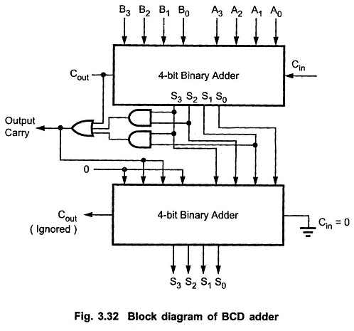
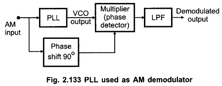
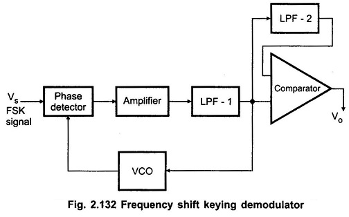
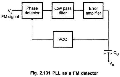
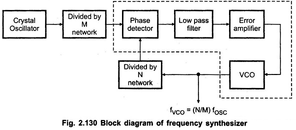
BCD Adder Circuit
BCD Adder Circuit | BCD Adder Truth Table | BCD Adder Block Diagram: The digital systems handles the decimal number in the form of binary coded decimal numbers (BCD). A BCD Adder Circuit that adds…
Combinational Circuit | Block Diagram | Design Procedure: When logic gates are connected together to produce a specified output for certain specified combinations of input variables, with no storage involved, the resulting circuit is called…
CMOS Inverter Working Principle: CMOS Circuit contain both NMOS and PMOS devices to speed the switching of capacitive loads. It consumes low power and can be operated at high voltages, resulting in improved noise immunity.…
Frequency Translator using PLL: The Frequency Translator means shifting the frequency of an oscillator by a small factor. Fig. 2.134 shows the block schematic for frequency translator using PLL. It consists of mixer, low pass…
AM Detection using PLL: AM Detection – A PLL can be used to demodulate AM signals as shown in the Fig. 2.133. The PLL is locked to the carrier frequency of the incoming AM signal.…
Frequency Shift Keying Demodulator Working (FSK): In digital data communication, binary data is transmitted by means of a carrier frequency. It uses two different carrier frequencies for logic 1 and logic 0 states of binary…
PLL FM Detector or Demodulator: The PLL can be very easily used as an FM detector or demodulator. Fig. 2.131 shows the PLL FM Detector or Demodulator Block Diagram. When the PLL is locked in…
Block Diagram of Frequency Synthesizer using PLL: The Block Diagram of Frequency Synthesizer using PLL that can produce a precise series of frequencies that are derived from a stable crystal controlled oscillator. The Fig. 2.130…
Frequency Multiplier using PLL 565: Fig. 2.128 shows the block diagram for a frequency multiplier using PLL 565. Here , a divide by N network is inserted between the VCO output (pin 4) and the…
IC 565 PLL | Pin Diagram | Block Diagram: IC 565 PLL is available in a 14 pin DIP package and 10 pin metal can package. Fig. 2.124 shows 14-pin package configuration for IC 565…