Hexadecimal Number System (Definition, Conversions & Examples)
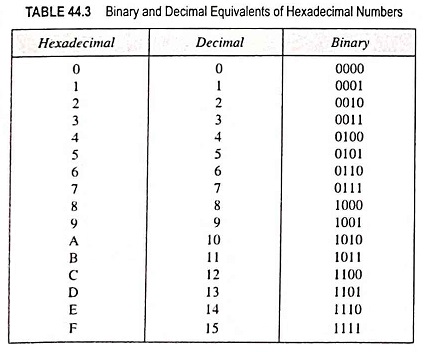
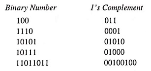
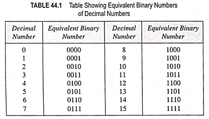
Hexadecimal Number System (Definition, Conversions & Examples): The binary number system forms the natural choice for the two-state systems. But in this system, the numbers tend to get short rather long. Hence to reduce the…
Comments Off on Hexadecimal Number System (Definition, Conversions & Examples)
October 29, 2022