BJT Transistor Articles:
Transistor Construction: The transistor construction consists of a silicon or germanium (preferably silicon because of its smaller cutoff current ICBO, smaller variations in ICBO due to variations in temperature and higher operating temperature) crystal in which a layer of N-type material is … (Read More)
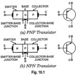
Transistor Terminals (Emitter, Collector and Base): As mentioned already, transistor is a single crystal in which there are two P-N junctions, as shown in Fig. 10.1. The idea behind is to have first section to supply the charges (either holes or … (Read More)
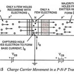
Transistor Action: Operation of PNP Transistor: Transistor action – Transistors of both types (P-N-P and N-P-N) behave exactly in the same way except change in biasing and majority carriers. In P-N-P transistors the conduction is by holes whereas in N-P-N … (Read More)
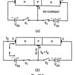
What is Transistor Biasing? – Types of Biasing As already mentioned, for normal operation of a transistor emitter-base junction is always forward biased and collector-base junction is always reverse biased. For a moment if the Transistor Biasing of emitter-base junction is … (Read More)
Important Points Regarding Working of Transistors: The noteworthy points regarding working of transistors are summarized below. 1. Current conduction in N-P-N transistor is by electrons and the conventional current flow will be in the opposite direction. Current conduction in P-N-P transistor is … (Read More)
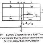
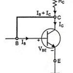
Explain Transistor Current Components: The various transistor current components which flow across the forward-biased emitter junction and reverse biased collector junction are indicated in Fig. 10.11. The current flowing into the emitter is referred to as the emitter current and designated … (Read More)
Current Amplification Factor: There are two current amplification factors, the alpha factor (α) and the beta factor (β) defined below : The alpha factor (α) is also called the current amplification factor and is the ratio of change in collector current (IC) … (Read More)
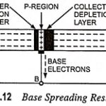
Base Spreading Resistance: With two depletion layers penetrating the base, the base holes are confined to the thin region of P-type semiconductor illustrated in Fig. 10.12. The resistance of this thin region (or section) is called the base spreading resistance rbb′. With … (Read More)
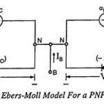
Ebers Moll Model for PNP Transistor: Device modelling aims at relating physical device parameters to device terminal characteristics. Device modelling is especially important for integrated circuits, since simple and accurate device models are required to predict the performance of a circuit. … (Read More)
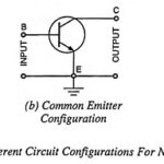
Transistor Circuit Configurations (CB, CE, CC): As already mentioned, a Transistor Circuit Configurations is a three-terminal device (having three terminals namely emitter, base and collector) but we require four terminals—two for the input and two for the output for connecting it … (Read More)
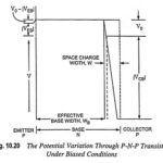
Early Effect and Base Width Modulation: In active region, the emitter-base (EB) junction is forward biased and collector-base (CB) junction is reverse biased, so the barrier width at EB junction is negligible in comparison with the space-charge width at CB junction, … (Read More)
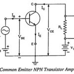
Transistor as an Amplifier – Circuit Diagram and Its Workings: The main utility of a transistor lies in its ability of amplifying weak signals. The weak signal is applied at the input terminals and the amplified output is obtained across the … (Read More)
Transistor Load Line Analysis (DC and AC Load Line and Q Point): The concept of Transistor load line analysis is very important in understanding the working of a transistor. It is defined as the locus of operating point on the output … (Read More)
Transistor Lead Identification and Testing: Transistor Lead Identification and Testing – After the transistor has been manufactured, as already discussed, leads of, typically, gold, aluminium, or nickel are then attached and the entire structure is encapsulated in a container such as … (Read More)
How to use a Transistor as a Diode – Working and Equation: The transistor can be modified to operate as a diode by short circuiting the two transistor terminals, as shown in Fig. 10.69 [collector and base terminals are shorted making … (Read More)
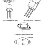
What is Thermal Runaway and Heat Sink? The maximum average power PC max which a transistor can dissipate depends upon the construction of the transistor and may lie in the range of a few milliwatts and 200 W. This maximum power … (Read More)
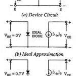
Transistor approximation (Ideal, Second and Higher): An NPN transistor is shown in Fig. 10.71 (a). Voltage appearing across the emitter diode is denoted by VBE and that appearing across the collector-emitter terminals is denoted by VCE. Ideal Approximation: An ideal approximation of … (Read More)
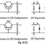
DC Equivalent Circuit of Transistor: DC Equivalent Circuit of Transistor – In the common base circuit, the emitter diode acts like a forward biased ideal diode, while collector diode acts as a current source because of transistor action. Thus an ideal transistor … (Read More)
What is BJT Beta Rule? Like transfer of primary and secondary winding impedances of a transformer, resistance from one part of a transistor circuit can be referred to another parts. For instance, resistance of collector circuit, RL can be referred to … (Read More)
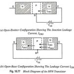
Leakage Current in a Transistor and Breakdown Voltage: Leakage Currents: In CB circuits shown in Fig. 10.77, if emitter current is made zero, the B-C junction still remains reverse biased and therefore, a reverse-bias leakage current exists in this junction, and … (Read More)