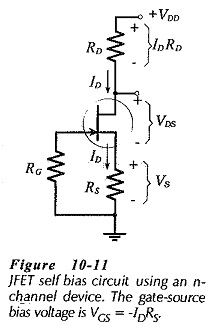
Self Bias Circuit Diagram
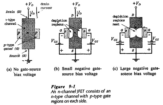
Self Bias Circuit Diagram: Circuit Operation - In a self bias JFET circuit, gate-source bias is provided by the voltage drop across a resistor in series with the device source terminal. Consider the n-channel JFET…
Comments Off on Self Bias Circuit Diagram
February 17, 2019