Circuits for Producing Impulse Waves:
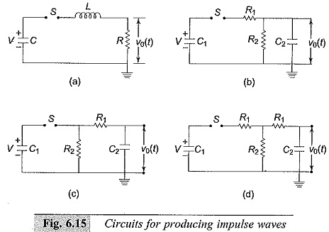
A double exponential waveform of the type mentioned in Eq. (6.15) may be produced in the laboratory with a combination of a series R-L-C circuit under over damped conditions or by the combination of two R-C circuits. Different equivalent circuits that produce impulse waves are given in Figs 6.15a to d. Out of these circuits, the ones shown in Figs 6.15a to 6.15d are commonly used. Circuit shown in Fig. 6.15a is limited to model generators only, and commercial generators employ circuits shown in Figs 6.15b to 6.15d.
A capacitor (C1 or C) previously charged to a particular d.c. voltage is by closing the switch S. The discharge voltage V0(t) shown in Fig. 6.15 gives the desired double exponential waveshape.
Analysis of Impulse Generator Circuit of Series R-L-C Type
Referring to Fig. 6.15 the current through the load resistance R is given by
with initial condition at t = 0 being i(0) = 0 and the net charge in the circuit q= 0. Writing the above equation as a Laplace transform equation,
The voltage across the resistor R (which is the output voltage) is, ν0(s) = I(s) R; hence,
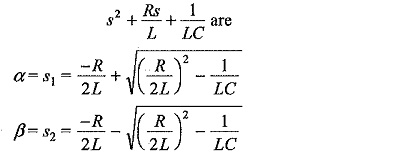
For an overdamped condition, R/2L≥1/√LC
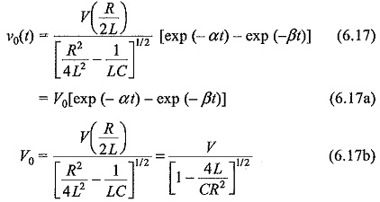
The solution of the equation for ν0(t) is
The wave front and the wave tail times are controlled by changing the values of R and L simultaneously with a given generator capacitance C; choosing a suitable value for L, β or the wave front time is determined and α or the wave tail time is controlled by the value of R in the circuit. The advantage of this circuit is its simplicity. But the waveshape control is not flexible and independent. Another disadvantage is that the basic circuit is altered when a test object which will be mainly capacitive id nature, is connected across the output. Hence, the waveshape gets changed with the change of test object.
Analysis of the Other Impulse Generator Circuits:
The most commonly used configurations for Impulse Waves generators are the circuits shown in Figs 6.15b and c. The advantages of these circuits are that the wave front and wave tail times are independently controlled by changing either R1 or R2 separately. Secondly, the test objects which are mainly capacitive in nature from part of C2.
For the configuration shown in Fig. 6.15b, the output voltage across C2 is given by
Performing Laplace transformation,
where i2 is the current through C2.
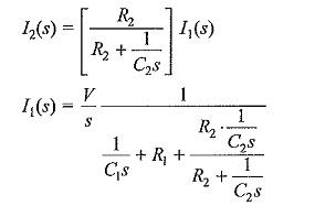
Taking the current through C1 as i1 and its transformed value as I1(s),
After simplification and rearrangement,
Hence, the roots of the equation
are found from the relations
Taking inverse transform of ν0(s) gives
Hence, the roots may be approximated as
Following a similar analysis, it may be shown that the output waveform for the circuit configuration of 6.15c will be
where α and β are the roots of the Eq. (6.19). The approximate values of α and β given by Eq. (6.21) are valid for this circuit also.
The equivalent circuit given in Fig. 6.I5d is a combination of the configurations of Fig. 6.15b and Fig. 6.15c. The resistance R1 is made into two parts and kept on either side of R2 to give greater flexibility for the circuits.
Restrictions on the Ratio of the Generator and Load Capacitances, C1/C2 on the Circuit Performance
For a given waveshape, the choice of R1 and R2 to control the wave front and wave tail times is not entirely independent but depends on the ratio of C1/C2. It can be shown mathematically that
where y = C1/C2 and P and Q are functions ofy. In order to get real values for R1 and R2 for a given waveshape a maximum and minimum value of ν exists in practice. This is true whether the configuration of Fig. 6.15b or 6.15c is used. For example, with the circuit of Fig. 6.15b, the ratio of C1/C2 cannot exceed 3.35 for a 1/5 μs waveshape. Similarly, for a 1/50 μs waveshape the ratio C1/C2 lies between 6 and 106.5. If the configuration chosen is 6.15c, the minimum value of Ci/C2 for 1/5 μs waveshape is about 0.3 and that for the 1/50 μs waveshape is about 0.01. The reader is referred to High Voltage Laboratory Techniques by Craggs and Meek for further discussion on the restrictions imposed on the ratio C1/C2.
Effect of Circuit Inductances and Series Resistance on the Impulse Generator Circuits
The equivalent circuits shown in Figs 6.15a to d, in practice comprise several stray series inductances. Further, the circuits occupy considerable space and will be spread over several metres in a testing laboratory. Each component has some residual inductance and the circuit loop itself contributes for further inductance. The actual value of the inductance may vary from 10 μH to several hundreds of microhenries. The effect of the inductance is to cause oscillations in the wave front and in the wave tail portions. Inductances of several components and the loop inductance are shown in Fig. 6.16a. Figure 6.16b gives a simplified circuit for considering the effect of inductance. The effect of the variation of inductance on the waveshape is shown in Fig. 6.16c. If the series resistance R1 is increased, the wave front oscillations are damped, but the peak value of the voltage is also reduced. Sometimes, in order to control the front time a small inductance is added.
Impulse Generators for Testing Objects having Large Capacitance
When test objects with large capacitances are to be tested (C > 5 nF), it is difficult to generate standard Impulse Waves with front time within the specified tolerance off ±30% and the specified less than 5% tolerance in the overshoot. This is mainly because of the effect of the inductance of the impulse generator and the front resistors. Normally the inductance of the Impulse Waves generator will be about 3 to 5 μH per stage and that of the leads about 1 μH/m. Also the front resistor which is usually of bifilar type, has inductance of about 2 μH/m.


