Class B Push Pull Amplifier – Circuit Diagram, Operation and Derivation:
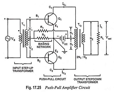
The circuitry for the Class B Push Pull Amplifier operation is the same as that for the class A operation except that the devices are biased at cutoff. The transistor circuit of Fig. 17.25 operates as class B if R2 = 0 because a transistor is essentially at cutoff if the base is shorted to the emitter.
The advantages of class B operation over class A operation are given below :
- It is possible to obtain greater power output—class B push pull amplifier provides practically 4-times the power supplied by a single ended amplifier provided load resistance remains the same.
- It gives higher operating efficiency (theoretical 78.5%). It is primarily due to the fact that no power is drawn by the circuit under zero signal condition.
Because of above advantages, a push-pull class B transistor circuit is preferred in systems where the power supply is limited, such as those operating from solar cells or a battery. The automatic cancellation of all even-order harmonics from the output makes class B push pull amplifier highly desirable for communication sound equipment.
The drawbacks of class B push pull amplifiers are that the harmonic distortion is higher, self-bias cannot be used, and the supply voltages must have good regulation.
class B push pull amplifier are widely employed for audio work in portable record-players, as stereo amplifiers and in high-fidelity radio receivers.
Circuit Arrangement:
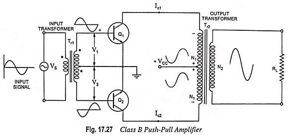
Circuitry for a class B push pull amplifier is shown in Fig. 17.27. As illustrated in the figure, the bases of the two CE-connected identical transistors Q1 and Q2 have been connected to the opposite ends of the secondary of the input transformer Tr1. Load resistance RL is coupled to the collector terminals of the two transistors through output transformer Tr2. The emitter terminals of the transistors are connected to the centre tap of the secondary of the input transformer Tr1 while the supply VCC is connected to the centre tap on the primary of output transformer. This is done in order to have balanced circuits. Since zero bias is required for cutoff, the two bases of the two transistors have been grounded.
Circuit Operation:
When the input signal is applied, the centre tapped secondary of the input transformer develops two signals which are identical but in phase opposition. The transistors, Q1 and Q2 are driven by these two signals. Thus when V1 is going positive, V2 is going negative, so that transistor Q2 is being biased further off when transistor Q1 is being biased on. As the collector current in Q1 increases from zero, it produces a half sine wave of voltage across the upper half of the primary of the output transformer, as shown. When the positive half cycle of the input signal to Q1 begins to go negative, the signal at Q2 base is commencing to go positive. Thus, as Q1 becomes biased off again, Q2 is biased on and a half cycle of voltage waveform is generated across the lower primary winding of output transformer.
The effect of the two half cycles in separate halves of the primary of output transformer is to produce a magnetic flux in the transformer core, which flows first in one direction and then in the opposite direction. This flux links with the secondary of the output transformer and generates a complete sine wave output, which is passed on to the load. In the class B circuit, the two output transistors are said to be operating in push-pull.
As explained above, a full sine wave is developed at the output of the transformer. When no signal is present, both transistors remain off, and thus no current is drawn from dc supply source VCC. Hence there is no dissipation of power with zero signal. Some power is dissipated in each transistor only while the transistor is conducting.
The load resistance (usually a loudspeaker) is connected across the secondary of the output transformer. The turn-ratio 2N1 : N2 of the transformer is chosen so that load resistance RL is matched with the output impedance of the transistor. Under matched conditions, maximum power is delivered to the load by the amplifier.
Conversion Efficiency of Class B Amplifier:
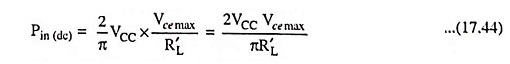
The power provided to the load RL coupled to the amplifier is drawn from the dc power supply VCC and is considered an input dc power. The input dc power is given as
![]()
where Idc is the average or direct current taken from the dc supply VCC.
In class B operation the current drawn from a single power supply is a full-wave rectified signal, thus

Thus,
![]()
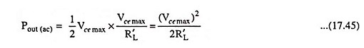
AC power output,

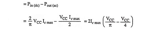
Total collector power dissipation for the two transistors,
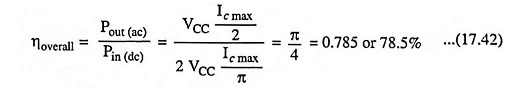
Overall efficiency,
Relation Between Maximum Output Power and Transistor Dissipation:
In class B operation dc power input is given by Eq. (17.40) i.e.,
![]()
Since

where R′L is reflected load resistance
So,
AC power output,

Substituting Ic max = Vce max/R′L from Eq. (17.43) in above equation, we have
Total collector power dissipation for the two transistors

Above Eq. (17.46) indicates that the collector dissipation is zero at no signal (i.e., Vce max = 0), rises as Vce max increases and passes through a maximum when Vce max = 2VCC/π. The peak dissipation is determined by substituting Vce max = 2VCC/π in above Eq. (17.46).

The maximum power which can be delivered is obtained by substituting Vce max = VCC (for Vc min = 0)
So,
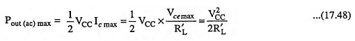
Comparing Eqs. (17.47) and (17.48), we have

The above expression is for maximum power dissipation in both transistors. Maximum power dissipation per transistor is 0.2 times maximum ac power output.