Darlington Pair Transistor – Circuit Diagram and its Workings:
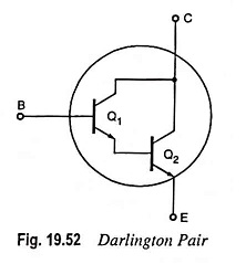
A very popular connection of two BJTs for operation as one “superbeta” transistor is the Darlington connection. In practice, the two transistors are put inside a single package and three terminals E, B and C are brought out, as depicted in Fig. 19.52. The main feature of the Darlington Pair Transistor connection is that the composite transistor acts as a single unit that has a high current gain (product of the current gains of the individual transistors) and high input impedance. The current gain provided by the Darlington connection is of the order of a few thousand.
Analysis:
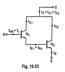
Let β1 and β2 be the dc values of transistors Q1 and Q2 respectively. Then by definition.
Collector current of transistor Q1,
and Emitter current of transistor Q1,
Base current of transistor Q2,
So collector current of transistor Q2,
Now collector current,
Effective β of Darlington Pair Transistor connection
From above Eq. (19.94) it is obvious that the effective β of the Darlington connection is product plus the sum of the βs of the individual transistors. It is usually true that β1β2 >> (β1 + β2) so
Darlington Pair Transistor are often fabricated on a single chip to achieve matched transistors Q1 and Q2 characteristics. For β1 = β2 = β, we have the effective β of the Darlington connection
It is assumed that the dc and small signal values of β are approximately equal.
Determination of Small-Signal Input Resistance From B to E, rin(DP), and The Emitter Resistance r′e(DP), of The Composite Transistor
We know that
AC resistance looking into the base of transistor Q2,
Now
Since IE2 = β2IB2 = β2IE1, we have
Substituting IE1 = IE2/β2 in Eq. (19.99) we have
The total effective resistance looking into the base of transistor Q1, (across the composite B-E terminals), i.e. the effective small-signal input resistance of the Darlington connection,
Substituting r′e1 = β2r′e2 from Eq. (19.100) we have
Since βDP ≈ β1β2, the effective emitter resistance


