Differential Amplifier Circuit Operation:
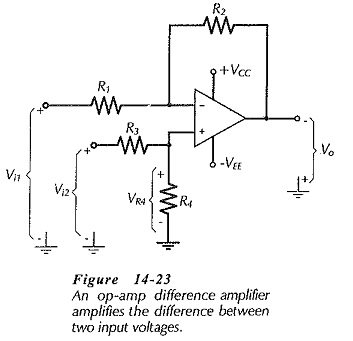
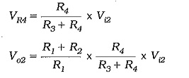
A Differential Amplifier Circuit Operation amplifies the difference between two inputs. The circuit shown in Fig. 14-23 is a combination of inverting and noninverting amplifiers. Resistors R1, R2, and the op-amp constitutes an inverting amplifier for a voltage (Vi1) applied to R1. The same components (R1, R2, and the op-amp) also function as a noninverting amplifier for a voltage (VR4) at the noninverting input terminal. It is seen that VR4 is derived from input voltage Vi2 by the voltage divider R3 and R4.
To understand the Differential Amplifier Circuit Operation, consider the output produced by each input voltage when the other input is zero:
with Vi2 = 0,
with R3 = R1, and R4 = R2,
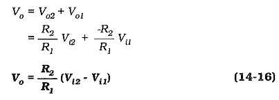
When both inputs are present,
When R2 = R1, the output voltage (as calculated by Eq. 14-16) is the direct difference between the two inputs. With R2 greater than R1, the output becomes an amplifier version of (Vi2 – Vi1).
Input resistances:
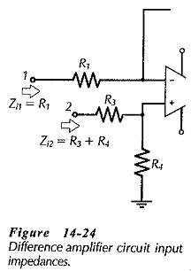
Consider the input portion of the Differential Amplifier Circuit Operation reproduced in Fig. 14-24. The resistance at input terminal 1 is the same as the input impedance for an inverting amplifier: Zi1 = R1. The input resistance at the op-amp noninverting input terminal, is very high (as in the case of a noninverting amplifier), and this is in parallel with resistor R4. So, the input impedance at terminal 2 in Fig. 14-24 is Zi2 = R3 + R4.
Equation 14-16 was derived by assuming that R3 = R1, and R4 = R2. It can be shown that the same result is obtained when the ratio R4/R3 equals R2/R1, so that the actual resistor values do not have to be equal For equal resistances at the two input terminals
Then, calculate the resistances of R3 and R4 from,
A simple rule-of-thumb can be used for determining suitable resistance values for R3 and R4 when the two input resistances do not have to be exactly equal. Select, R4 = R2/ACL; which always makes R4 = R1. Then, calculate R3 as, R3 = R1/ACL.
Common Mode Voltages:
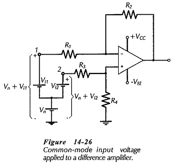
A common-mode input voltage is a signal voltage (dc or ac) applied to both input terminals at the same time. This is illustrated in Fig. 14-26, where Vi1, Vi2, and the common-mode voltage (Vn) are all represented as inputs from dc sources. As shown, the input voltages at terminals 1 and 2 are changed from Vi1 and Vi2 to (Vn + Vi1) and (Vn + Vi2).
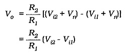
Equation 14-16 shows that the output voltage is the amplified difference between the two input voltages. So,
This shows that the common-mode input is completely cancelled. However, recall that the gain equation depends upon the resistor ratios (R4/R3 and R2/R1) being equal If the ratios are not exactly equal, one input will experience a larger amplification than the other. Also, the common-mode voltage at one input terminal will be amplified by a larger amount than that applied to the other input terminal. In this case, common-mode inputs will not be completely cancelled.
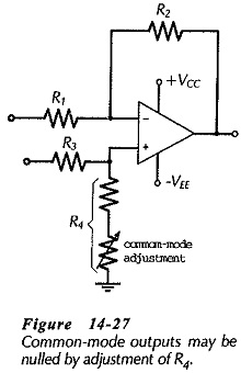
Because it is difficult to perfectly match resistor ratios (especially for standard-value components), some common-mode output voltage is almost certain to be produced where a common-mode input exists. Figure 14-27 shows a circuit modification for minimizing common-mode outputs from a difference amplifier. Resistor R4 is made up of a fixed-value resistor and a small-value adjustable resistor connected in series. This provides adjustment of the ratio R4/R3 to match R2/R1, so that common-mode outputs can be nulled to zero.
