Differential Amplifiers Articles:
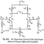
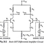
Dual Input Balanced Output Differential Amplifier: The dual input balanced output differential amplifier configuration is shown in Fig. 20.2. In the given circuit two input signals vin1 and vin2 are applied to the bases B1 and B2 of transistors Q1 and Q2. … (Read More)
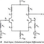
Dual Input Unbalanced Output Differential Amplifier: It is an important configuration and converts dual inputs into a single ended output. In this configuration, two input signals are applied and the output is measured at only one of the two collectors (either … (Read More)
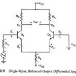
Single Input Balanced Output Differential Amplifier: In a single input balanced output differential amplifier an input signal is applied to either input, with the other input connected to ground. However, due to the common-emitter connection the input signal operates both transistors, … (Read More)
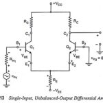
Single Input Unbalanced Output Differential Amplifier: Single input unbalanced output differential amplifier configurations are rarely used. The reasons for this are as follows: This configuration is identical to the CE amplifier but it needs comparatively more components and yields less voltage gain … (Read More)
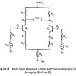
Swamping Resistor in Differential Amplifier: The dependence of the voltage gain of the differential amplifiers on variations in ac emitter resistance r′e can be reduced and also the linearity range of the differential amplifiers can be increased if external resistors R′E … (Read More)
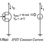
Constant Current Source in Differential Amplifier: An ideal current source provides a constant current regardless of the load connected to it. There are many applications in electronics for a circuit that provides a constant current with a very high impedance. Constant … (Read More)
Constant Current Bias in Differential Amplifier: In the differential amplifiers discussed so far, we have used the combination of RE and VEE to produce emitter dc bias current. Alternatively, constant current bias circuit can also be employed to set up the … (Read More)
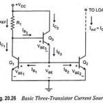
What is Current Mirror? – Circuit Diagram and its Workings: The two-transistor current source, also called a current mirror, is the basic building block in the design of integrated circuit current sources. Figure 20.25 (a) depicts the basic current-source circuit, which … (Read More)
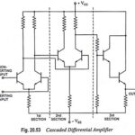
Cascaded Differential Amplifier Working Principle: Cascaded Differential Amplifier Working Principle – Figure 20.53 gives an idea of how differential amplifiers can be cascaded to give an op-amp. Here the output of first section differential amplifier is fed to the second section, … (Read More)
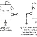
JFET Differential Amplifier – Circuit Diagram and its Workings: Many differential amplifiers are constructed with FETs because of the large impedance they present to the input signals—an exceptionally important property in many applications, including operational amplifiers and instrumentation amplifiers. A large … (Read More)
Voltage Level Translator (Level Shifter): Voltage Level Translator (Level Shifter) is usually an emitter follower circuit which is used to shift the dc level at the output of the intermediate stage downward to zero volt w.r.t. ground. The level translator should be … (Read More)
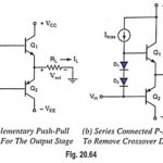
Output Stage of an Op Amp and its Voltage Transfer Characteristics: The output stage of an op amp is another requirement which should have very small output impedance and provide the external load current so that large output voltage swing is … (Read More)