Differentiator using Op Amp:
A Differentiator using Op Amp circuit that performs the mathematical operation of differentiation. It produces an output voltage proportional to slope of the input voltage. A common application of a differentiator is the detection of the leading and trailing edges of rectangular pulse.
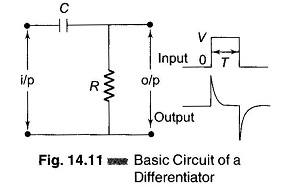
Figure 14.11 shows a basic CR differentiator. If a rectangular pulse is applied, the output of the circuit is positive and negative spikes. The positive spike occurs at the same instant as the leading edge of the input and the negative spike at the same instant as the trailing edge.
When the input voltage changes from 0 to V, the capacitor begins to charge exponentially, and the output voltage suddenly jumps from 0 to V (after 5 time constants, the capacitor voltage is within 1% of its final voltage V) and then decays exponentially.
Over the trailing edge of a pulse, the input voltage steps negatively and we get a negative spike. For a CR Differentiator to produce narrow spikes the time constant must be 10 times smaller than period T.
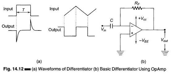
In Fig. 14.12 (b), when the input voltage varies, the capacitor charges or discharges. Because of the virtual ground, the capacitor current passes through the feedback resistor, producing a voltage. This voltage is proportional to the slope of the input voltage.
A rectangular input, shown in Fig. 14.12 (a), is used to obtain positive and negative spikes. The leading edge of the pulse is approximately a positive ramp, so that the output is a negative spike of very short duration. Similarly, the trailing edge of the input pulse is approximately negative ramp, so that the output is a very narrow positive spike. Similarly, if a triangular waveform is given as input, a square waveform is obtained at the output.
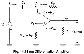
A basic differentiator using Op Amp is constructed from a basic inverting amplifier by replacing the input resistor R1 by a capacitor C1 as shown in Fig. 14.13. Using Kirchoff’s current equation at node V2 is Ic = Ib + If. Since Ib ≡ 0,
But
and
As
But V1 = V2 = 0, because A is very large therefore
From the above equation it can be seen that a differentiator performs the opposite function of integration. If a cosine wave is applied as the input, a sine wave will be produced at the output, and a triangular wave as the input will produce a square wave at the output.
The Differentiator using Op Amp of Fig. 14.13 has a tendency to oscillate which is undesirable.
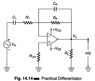
The gain RF/XC1 of the circuit increases at a rate of 20 db/decade with increases in frequency, which makes the circuit unstable. As the frequency increases, the input impedance (XC1) decreases, making the circuit more susceptible to high frequency noise. This noise is superimposed after amplification, on the differentiated output signal. This high frequency noise and stability can be corrected by the use of R1 and CF, as shown in Fig. 14.14, which is a practical differentiator.
A typical value for R1 is between 0.01RF and 0.1RF. With this the closed loop voltage gain is reduced (to between -10 and -100).
The differentiating circuit is most commonly used in wave shaping circuits to detect high frequency components in an input signal and as a rate of change detector in FM modulators. It is also used in triggering the time base generator in an oscilloscope.
To design a practical differentiator using Op Amp the following parameters are required.
(a) fa is the highest frequency range to be differentiated, and is given by fa = 1/(2πRFC1).
(b) fb is the gain limiting frequency at which the gain begins to decrease at a rate of 20 db/decade. This frequency is given by fb = 1/2πR1C1, where R1C1 = RFCF and fb = 20 fa.


