Digital Integrated Circuits Articles:
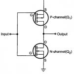
CMOS Inverter Working Principle: CMOS Circuit contain both NMOS and PMOS devices to speed the switching of capacitive loads. It consumes low power and can be operated at high voltages, resulting in improved noise immunity. Fig. 3.1 shows the basic CMOS Inverter … (Read More)
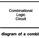
Combinational Circuit | Block Diagram | Design Procedure: When logic gates are connected together to produce a specified output for certain specified combinations of input variables, with no storage involved, the resulting circuit is called Combinational Logic. In Combinational logic, the output … (Read More)
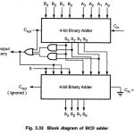
BCD Adder Circuit | BCD Adder Truth Table | BCD Adder Block Diagram: The digital systems handles the decimal number in the form of binary coded decimal numbers (BCD). A BCD Adder Circuit that adds two BCD digits and produces a … (Read More)
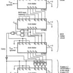
BCD Subtraction: Addition of signed BCD numbers can be performed by using 9’s or 10’s complement methods. A negative BCD number can be expressed by taking the 9’s or 10’s complement. Let us see BCD Subtraction using 9’s Complement and BCD … (Read More)
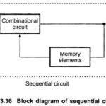
Sequential Circuits: There are many applications in which digital outputs are required to be generated in accordance with the sequence in which the input signals are received. This requirement cannot be satisfied using a combinational logic system. These applications require outputs … (Read More)
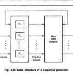
Sequence Generator in Digital Electronics: A Sequence Generator in Digital Electronics which generates a prescribed sequence of bits, in synchronism with a clock, is referred to as a sequence generator. Fig. 3.58 shows the basic structure of a sequence generator using … (Read More)
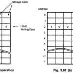
What is Semiconductor Memory? Memories are made up of registers. Each register in the memory is one storage location. Each location is identified by an address. The number of storage locations can vary from a few … (Read More)
ROM Memory: It is a read only memory. We can’t write data in this ROM Memory. It is non-volatile memory i.e. it can hold data even if power is turned off. Generally, Read Only Memory is used to store the binary … (Read More)
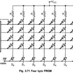
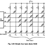
Programmable Read Only Memory (PROM): Fig. 3.71 shows four byte Programmable Read Only Memory (PROM). It has diodes in every bit position; therefore, the output is initially all 0s. Each diode, however has a fusible link in series with it. By addressing … (Read More)
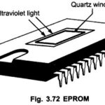
Erasable Programmable Read Only Memory (EPROM): Erasable Programmable Read Only Memory (EPROM) use MOS circuitry. They store 1s and 0s as a packet of charge in a buried layer of the IC chip. EPROMs can be programmed by the user with … (Read More)
EEPROM (Electrically Erasable Programmable Read Only Memory): Electrically Erasable Programmable Read Only Memory (EEPROM) also use MOS circuitry very similar to that of EPROM. Data is stored as charge or no charge on an insulated layer or an insulated floating gate … (Read More)
NVRAM (Non Volatile Random Access Memory): It is Non Volatile Ram. It created by the combination of a static RAM and an electrically erasable PROM (EEPROM) in the same chip. The EEPROM and static RAM … (Read More)
What is Flash Memory in Digital Electronics? Flash Memory in Digital Electronics (sometimes called “flash RAM”) is a type of constantly-powered nonvolatile memory that can be erased and reprogrammed in units of memory called Blocks. It is a variation of electrically … (Read More)
What is RAM? Unlike ROM, we can read from or write into the RAM, so it is often called read/write memory. The numerical and character data that are to be processed by the computer change frequently. These data … (Read More)
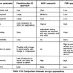
Design of Digital Circuits: We have seen the design of digital circuits using fixed function ICs. There are two more approaches for the Design of Digital Circuits. Use of application specific integrated circuits (ASICs) Use of programmable logic devices (PLDs) In the fixed function … (Read More)
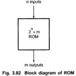
Read Only Memory (ROM): A Read Only Memory (ROM) is a device that includes both the decoder and the OR gates within a single IC package. The Fig. 3.82 shows the block diagram of ROM. It consists of n input lines … (Read More)
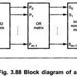
Programmable Logic Array (PLA) | Block Diagram of PLA: The combinational circuit do not use all the minterms every time. Occasionally, they have don’t care conditions. Don’t care condition when implemented with a ROM becomes an address input that will never … (Read More)
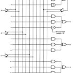
Programmable Array Logic (PAL): We have seen that PLA device with a Programmable AND array and Programmable OR array. However, Programmable Array Logic (PAL) is a programmable logic device with a fixed OR array and a programmable AND array. Because only … (Read More)
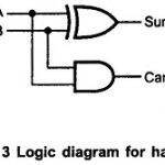
Half Adder and Full Adder Circuit: Adders are divided into two categories namely, half adder and full adder circuit. Half Adder Circuit: The Half Adder Circuit operation needs two binary inputs : augend and addend bits; and two binary outputs : sum and … (Read More)
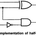
Half Subtractor and Full Subtractor Circuit: Subtractor are divided into two categories namely, half subtractor and full subtractor circuit. Half Subtractor Circuit: The Half Subtractor Circuit consists of four possible elementary operations, namely, In all operations, each subtrahend bit is subtracted from the minuend … (Read More)
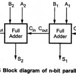
Parallel Adder and Subtractor: Parallel Adder and Subtractor which consists of three categories, namely, n Bit Parallel Adder,Binary Parallel Adder and n Bit Parallel Subtractor. n Bit Parallel Adder: We have seen, a single full-adder is capable of adding two one-bit numbers … (Read More)
CMOS NAND Gate Circuit Diagram: Fig. 3.3 shows CMOS NAND Gate Circuit Diagram 2-input NAND gate. It consists of two P-channel MOSFETs, Q1 and Q2, connected in parallel and two N-channel MOSFETs, Q3 and Q4 connected in series. P-channel MOSFET is ON … (Read More)
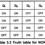
CMOS NOR Gate Circuit: Fig. 3.4 shows 2-input CMOS NOR Gate Circuit. Here, P-channel MOSFETs Q1 and Q2 are connected in series and N-channel MOSFETs Q3 and Q4 are connected in parallel. Like NAND circuit, this circuit can be analyzed by realizing that a … (Read More)
Performance of CMOS Gates: The Performance of CMOS Gates which based on following different categories namely, Operating Speed : Slower than TTL series. Approximately 25 to 100 ns depending on the subfamily of CMOS Inverter Circuit. It also depends on the power … (Read More)
Synchronous Sequential Circuits or Clocked Sequential Circuits: In Synchronous Sequential Circuits or clocked sequential circuits, clocked flip-flops are used as memory elements, which change their individual states in synchronism with the periodic clock signal. Therefore, the change in states of flip-flops … (Read More)