FET Transistor Articles:
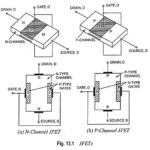
Junction Field Effect Transistor (JFET) – Construction, Symbols and Operation: Depending upon the majority charge carriers, Junction Field Effect Transistor (JFET) have been classified into two types, namely (i) N-channel JFETs with electrons as the majority charge carriers and (ii) P-channel … (Read More)
Advantages and Disadvantages of JFET: Junction field-effect transistors combine several merits of both conventional (or bipolar) transistors and vacuum tubes. Some of these advantages and disadvantages of JFET are enumerated below : 1. Its operation depends upon the flow of majority carriers … (Read More)
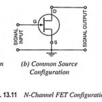
FET Configurations: FETs (JFETs and MOSFETs) have three configurations just as BJTs have. The three FET Configurations—the common gate, common source, and common drain configuration have been given in Fig. 13.11. Input and output terminals of different configurations have been given in … (Read More)
JFET Temperature Effects: The JFET, like other solid state devices, is subject to the JFET Temperature Effects. However, it is possible to bias the JFET such that it will exhibit a zero temperature coefficient i.e. drain current ID will be independent … (Read More)
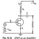
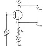
JFET as an Amplifier: One of the applications of JFET as an Amplifier of input signal. In FET the weak signal is applied between gate and source and an amplified output is taken across the drain-source circuit having load, as shown in … (Read More)
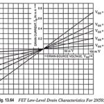
Parameters of JFET: JFET has certain parameters which determine the performance. Such Parameters of JFET are (i) ac drain resistance, (ii) transconductance, (iii) amplification factor, and (iv) dc drain resistance, as explained below: 1. AC Drain Resistance: It is defined as the … (Read More)
DC Load Line and Bias Point of FET Circuit: The DC Load Line and Bias Point for a FET circuit is drawn upon the output characteristics of the device in exactly the same way as for a BJT circuit. Consider the FET … (Read More)

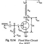
FET Biasing Methods – Fixed Bias, Self Bias, Potential Divider Bias and Current Source Bias: Unlike BJTs, thermal runaway does not occur with FETs. However, the wide differences in maximum and minimum transfer characteristics make ID levels unpredictable with simple fixed-gate … (Read More)
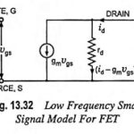
Small Signal Model of FET: The Small Signal Model of FET which consists of Low Frequency Small Signal Model for FET and High Frequency Model for FET. Low Frequency Model: In a FET, instantaneous drain current iD is a function of the … (Read More)
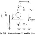
Common Source JFET Amplifier with AC Equivalent Circuit: The Common Source JFET Amplifier Circuit configuration is the most widely employed configuration. It is because this configuration provides high input impedance, good voltage gain and moderate output impedance. The circuit of a common … (Read More)
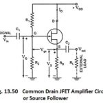
Common Drain JFET Amplifier or Source Follower: In the Common Drain JFET Amplifier circuit (also called the source follower), the output voltage is developed across source resistor RS. External load resistor RL is connected to FET source terminal S through coupling … (Read More)
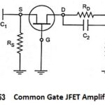
Common Gate JFET Amplifier and its AC Equivalent Circuit: The circuit of a simple Common Gate JFET Amplifier is shown in Fig. 13.53 and its ac equivalent circuit is shown in Fig. 13.54. In this Amplifier Circuit, input signal is applied … (Read More)
Generalized FET Amplifier Circuit: The analysis of a common source amplifier with a source resistance RS, a common gate amplifier and a common drain amplifier at low frequencies may be made by considering the Generalized FET Amplifier Circuit given in Fig. … (Read More)
Applications of FETs (Field Effect Transistors): Applications of FETs – FET has a very high input impedance (100 MΩ in case of JFETs and 104 to 109 MΩ in case of MOSFETs), the major shortcomings of an ordinary transistor i.e., low input … (Read More)
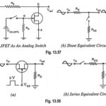
FET as a Voltage Variable Resistor (VVR): FET is a device that is usually operated in the constant-current portion of its output characteristics. But if it is operated in the region prior to pinch-off (i.e., where VDS is small, say below … (Read More)
Metal Insulator Semiconductor Field Effect Transistors (MISFETs): The Metal Insulator Semiconductor Field Effect Transistors (MISFETs) is one of the most widely used electronic devices, particularly in digital circuits, because of relatively small size-thousands of devices can be fabricated in a single … (Read More)
Depletion Type MOSFET – Construction, Operation and Characteristics: As we know already that when the gate is biased negative w.r.t. the source in an N-channel JFET, the depletion-region widths are increased. The increase in the depletion regions reduces the channel thickness, … (Read More)
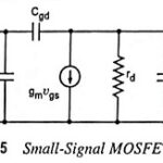
Small Signal Model of MOSFET: If the small bulk resistances of the source and drain are neglected, the Small Signal Model of MOSFET and its equivalent circuit between terminals G (G1), S, and D is identical with that for the JFET … (Read More)
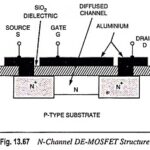
Enhancement Type MOSFET – Construction, Operation and Characteristics: Although DE-MOSFET is useful in special applications, it does not enjoy widespread use. However, it played an important role in history because it was part of the evolution towards the E-mode MOSFET, a … (Read More)
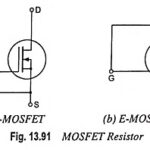
What is MOSFET Resistor? DE-MOSFET can be employed as a resistor by connecting the gate to the source, as shown in Fig. 13.91 (a), so that gate-tosource voltage VGS is zero. E-MOSFET may also be employed as a resistor by connecting the gate … (Read More)
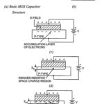
What is MOS Capacitor? The metal-oxide-semiconductor MOS capacitor shown in Fig. 13.92 (a) is the heart of the MOSFET. The metal may be aluminium or some other type of metal. In most cases, the metal is replaced by a high-conductivity polycrystalline … (Read More)
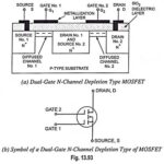
Dual Gate MOSFET – N Channel Depletion Type MOSFET: Cross view of a dual-gate N-channel depletion type MOSFET is shown in Fig. 13.93. It acts as if two FETs are connected in series, as is obvious from Fig. 13.93. The middle block … (Read More)
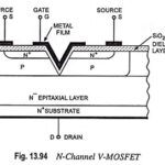
N Channel Power MOSFETs or V-MOSFET or V-FET: N Channel Power MOSFETs – Power MOSFETs are usually constructed in V-configuration, as shown in Fig. 13.94. That is why, the device is sometimes called the V-MOSFET or V-FET. V-shaped cut penetrates from the … (Read More)
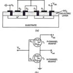
Complementary Metal Oxide Semiconductor (CMOS): With active load switching, the current drain with a low output is approximately equal to ID(sat). This may cause a problem with battery operated equipment. One way to reduce the current drain of a digital circuit … (Read More)
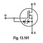
What is MOSFET Handling? MOSFET requires very careful handling particularly when out of circuit. In circuit, a MOSFET is as rugged as any other solid-state device of similar construction and size. MOSFET has an ultra thin silicon … (Read More)