Input Output Interfacing Techniques:
The most of the microprocessors support isolated I/O system. It partitions memory from I/O, via software, by having instructions that specifically access (address) memory, and others that specifically access I/O. When these instructions are decoded by the microprocessor, an appropriate control signal is generated to activate either memory or I/O operation. In 8085, IO/M signal is used for this purpose. The 8085 outputs a logic ‘1’ on the IO/M line for an I/O operation and a logic ‘0’ for memory, operation. In 8085, it is possible to connect 64 Kbyte memory and 256 I/O ports in the system since 8085 sends 16 bit address for memory and 8 bit address for I/O. I/O devices can be Input Output Interfacing Techniques to an 8085A system in two ways :
-
I/O Mapped I/O
-
Memory mapped I/O
In I/O mapped I/O, the 8085 uses IO/M signal to distinguish between I/O read/write and memory read/write operations. The 8085 has separate instructions IN and OUT for I/O data transfer. When 8085 executes IN or OUT instruction, it places device address (port number) on the demultiplexed low order address bus as well as the high order address bus. In other words, we can say that higher order address bus duplicates the contents of demultiplexed low-order address bus, when 8085 microprocessor executes an IN or OUT instruction. For example, if the device address is 60H then the contents on A15 to A0 will be as follows :
Here, A8 follows A0, A9 follows A1 and so on, as shown below.
The instruction IN inputs data from an input device (such as keyboard) into the accumulator and the instruction OUT sends the contents of the accumulator to an output device such as LED display. These are two byte instructions. The second byte of the instruction specifies the address or the port number of an I/O device. As it is a byte, the address or port number can be any of the 256 combinations of eight bits, from 00H to FFH. Therefore, the 8085 can communicate with 256 different I/O devices. When we want to Input Output Interfacing Techniques, it is necessary to assign a device address or a port number. Before going to see this device address logic, we will examine how the 8085 executes IN and OUT instructions.
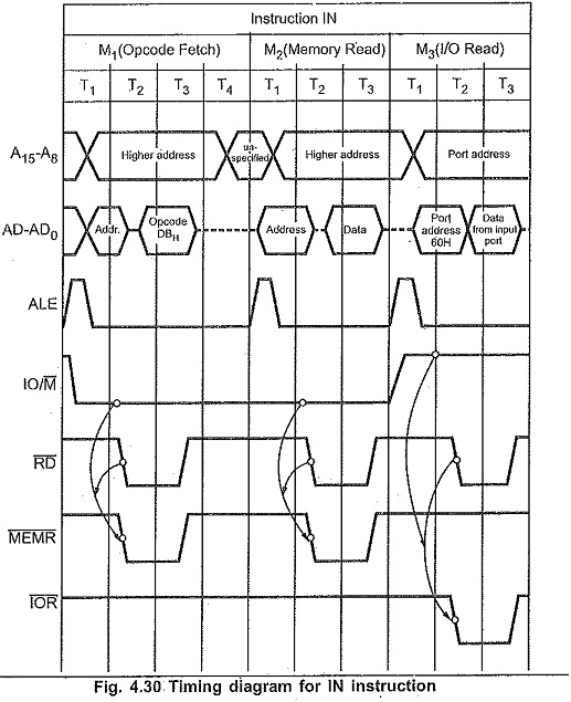
Fig. 4.30 shows the timing diagram of the IN instruction. It has three machine cycles. As usual, firSt cycle is opcode fetch machine cycle. The opcode fetch cycle is followed by one memory read machine cycle to read the address of port.
In the third machine cycle (I/O read) the 8085 microprocessor places the address of the input port on the low-order address bus AD7-AD0 as well as on the high-order address hubs A15-A8 and asserts the RD signal. During T2 and T3 of the machine cycle, RD and IO/M signals are 0 and 1 respectively, which activates IOR signal. The IOR signal enables the input port arid the data from the input port is placed on the data bus and transferred into the accumulator.
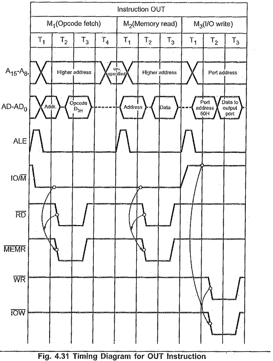
Fig. 4.31 shows the timing diagram of OUT instruction. It has, three machine cycles. The first machine cycle is an opcode fetch machine cycle, which reads the opcode of OUT instruction from the memory. The second machine cycle is a memory read machine cycle. This machine cycle reads the address of the port. In the third machine cycle (I/O write), the 8085 microprocessor places this address of the output port on the low-order address bus as well as on the high order address bus and asserts the WR signal. During T2 and T3 of the I/O write machine cycle, WR and ION signals are 0 and 1 respectively, which activates IOW signal. The IOW signal enables the output port and the data from the accumulator is sent to the output port.
I/O Device Selection:
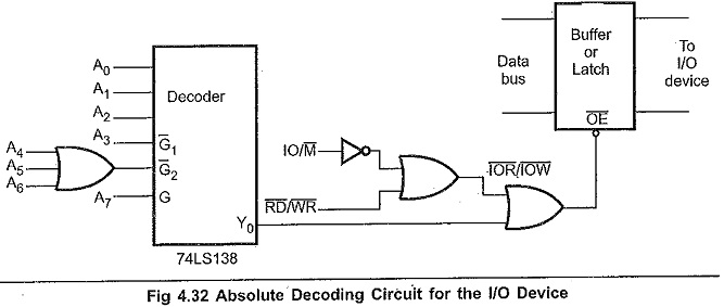
As mentioned earlier, the 8085 gives 8 bit I/O address. This means it can select one of the 256 I/O ports. To select an appropriate I/O device, it is necessary to do following things.
- Decode the address to generate unique signal corresponding to the device address on the bus.
- When device address signal and control signal (IOR or IOW) both are low, generate device select signal.
- Use device select signal to activate the Input Output Interfacing Techniques.
Interfacing Input Device :
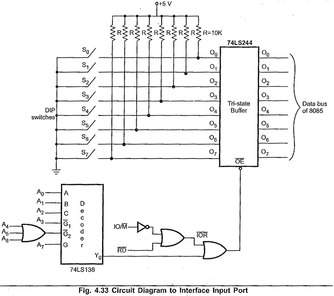
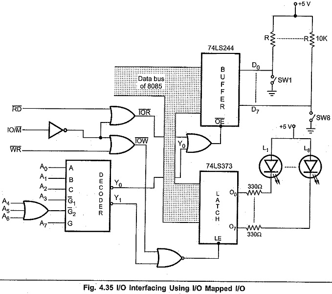
The microprocessor 8085 accepts 8 bit data from the input device such as keyboard, sensors, transducers etc. Fig. 4.33 (see Fig. on next page) shows the circuit diagram to Input Output Interfacing Techniques (buffer) which is used to read the status of 8 switches. The address for this input device is 80H as device select signal goes low when address is 80H.
When the switch is in the released position, the status of line is high otherwise status is low. With this information microprocessor can check a particular key is pressed or not.
The following program checks whether the switch 2 is pressed or not
Interfacing Output Device :
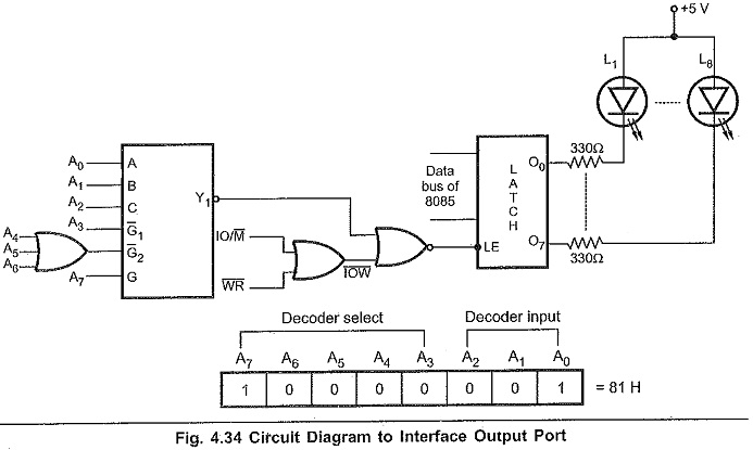
The microprocessor 8085 sends 8 bit data to the output device such as 7 segment displays, LEDs, printer etc. Fig 4.34 shows the circuit diagram to interface output port (latch) which is used to send the signal for glowing the LEDs. LED will glow when output pin status is low. The IC 74LS138 and 3 input OR gate is used to generate device select signal. The latch enable signal is active high. So NOR gate is used to generate latch enable signal, which goes high when Y1 and IOW both are low.
Memory Mapped I/O:
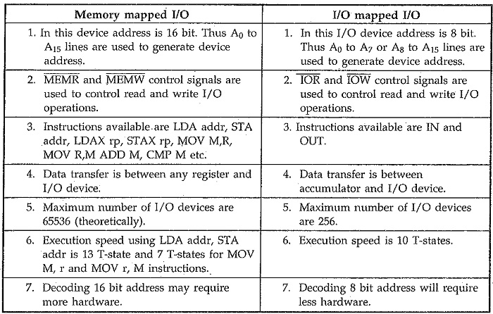
In memory mapped I/O, the I/O devices are assigned and identified by 16 bit addresses. The memory related instructions transfer the data between an I/O device and the microprocessor, as long as I/O port is assigned to the memory address space rather than to the I/O address space. The register associated with the I/O port is simply treated as a memory location. Thus I/O device becomes a part of the system’s memory map and hence its name. In memory-mapped I/O every instruction that refers to a memory location can control I/O. The source and destination of the data is limited with I/O mapped I/O, since for an IN instruction the destination register is always the accumulator, and for the OUT instruction the source register is always the accumulator. However, for memory mapped I/O there are number of sources and destinations.
Interfacing of I/O port with memory mapped I/O:
In memory mapped I/O, MEMR (memory read) and MEMW (memory write) control signals are required to control the data transfer between I/O device and microprocessor. As 8085 gives 16 bit memory address, it is necessary to decode 16 bit memory address to generate device select signal in case of memory mapped I/O. Fig. 4.36 shows the Input Output Interfacing Techniques devices in memory mapped I/O mode.


