Instruction Cycle of 8085 Microprocessor:
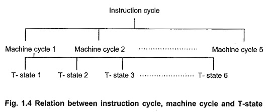
During normal operation, the microprocessor sequentially fetches, decodes and executes one instruction after another until a halt instruction (HLT) is executed. The fetching, decoding and execution of a single instruction constitutes an instruction cycle, which consists of one to five read or write operations between processor and memory or input/output devices. Each memory or I/O operation requires a particular time period, called machine cycle. In other words, to move byte of data in or out of the microprocessor, a machine cycle is required. Each machine cycle consists of 3 to 6 clock periods/cycles, referred to as T-states. Therefore we can say that, one Instruction Cycle of 8085 consists of one to five machine cycles and one machine cycle consists of three to six T-states i.e. three to six clock periods, as shown in the Fig. 1.4.
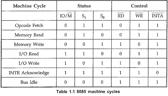
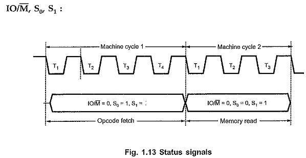
There are seven different types of machine cycles in the 8085A. Three status signals IO/M, S1 and S0 identify each type as shown in Table 1.1. These signals are generated at the beginning of each machine cycle and remained valid for the duration, of the cycle.
Representation of 8085 Signals and their Functions:
Before going to see the timing diagram, we will see the signals and their representation used in the timing diagrams.
Clock Signal:
The 8085 divides the clock frequency provided at X1 and X2 inputs by 2, which is called operating frequency. All the operations within the Instruction Cycle of 8085 are synchronized with this operating frequency. Therefore in the timing diagram operating frequency clock is shown on the top and then the signals are shown with reference to operating frequency . clock. Ideally, the clock signal should be square wave with zero rise time and fall time, as shown in the figure. But in practice, we don’t get zero rise time and fall time. Therefore the clock and other signals are always shown with finite rise and fall times. Fig. 1.5. shows the practical way of representing clock signal.
Single Signal:
Single signal is represented by a line. It may have status either logic 0 or logic 1 or tri-state. The change in the state of the signal takes finite time and hence the state change of signal is represented with finite rise time and fall time, as shown in the Fig. 1.6.
Group of Signals:
Group of signals is also called a bus e.g. address bus and data bus. To avoid complications in the timing diagram these signal are grouped and shown in the form of block as shown in Fig. 1.7.
In the group representation individual state is not considered, but the group state is considered. Change in state of single signal changes the state of group. It is represented by the cross as shown the Fig. 1.7. The tri-state condition of the group signals is shown by dotted lines. Two straight lines represent valid state/stable state.
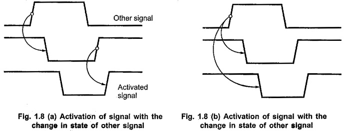
In microprocessor systems, activation of signal/signals depends on the state of other signal/signals. Such situations are shown in the timing diagrams with the help of specific symbols. There are four possibilities :
- Activation of a signal with the change in state of other signal.
- Activation of a signal with the Change in state of other signals.
- Activation of signals with the change in state of other signal.
- Activation of signals with the change in state of other signals.
Fig. 1.8 shows the representation of dependence of the signal/signals, in the timing diagram.
Signal Timings:
In the Instruction Cycle of 8085 microprocessor, signals are activated at specific instant for specific time period. Once we understand this, it is very easy to draw timing diagrams. The following section explains when the signals are activated and for what period they remain in active state.
ALE (Address Latch Enable):
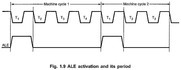
This signal is active high signal. It is activated in the beginning of the T1 state of each machine cycle, except bus idle machine cycle, and it remains active in the T1 state as shown in the Fig. 1.9.
A0—A7 (Lower byte address):
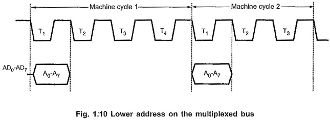
The lower byte of address is available on the multiplexed address/data bus (AD0 – AD7) during T1 state of each machine cycle, except bus idle machine cycle, as shown in Fig. 1.10.
D0-D7 (Data Bus):
The data from memory or I/O device and from microprocessor to memory or I/O device is transferred during T2 and T3-states. It is important to note that in read machine cycle, data will appear on the data bus during the later part of the T2-state, as shown in the Fig. 1.11, whereas in write cycle data will appear on the data bus at the beginning of the T2-state, as shown in the Fig. 1.11.
To read data from memory or I/O device it is necessary to select memory or I/O device. After selection, device will put the data from, selected location on the data bus. This action needs finite time. This time is referred to as ‘access time‘ . In case, of write cycle, data is available in the registers of the microprocessor and it can put that data on the data bus with zero access time.
A8 – A15 (Higher byte address):
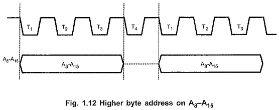
The higher byte of address is available on the A8 – A15 bus during T1, T2 and T3 — states of each machine cycle, except bus idle machine cycle, as shown in Fig. 1.12.
These signals are called status signals. They decide the type of machine cycle to be executed. They are activated at the beginning of T1-state of each machine cycle and remain active till the end of the machine cycle.
RD and WR:
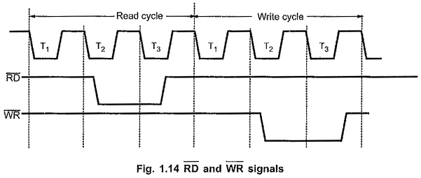
These signals decide the direction of the data transfer. When RD signal is active, data is transmitted from memory or I/O device to the microprocessor, and when WR signal is active, data is transmitted from microprocessor to the memory or I/O device. Both signals are never active at a time.
As we know data transfer in Instruction Cycle of 8085 takes place during T2 and T3, these signals are activated during T2 and T3, as shown in the Fig. 1.14.
