Instrumentation Amplifier Circuit Working:
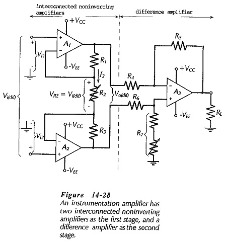
Circuit Operation – At first glance, the Instrumentation Amplifier Circuit Working in Fig. 14-28 looks complex, but when considered section by section it is found to be quite simple. First, note that the second stage (consisting of op-amp A3 and resistors R4 through R7) is a difference amplifier. Next, look at A1 and resistors R1 and R2; this is a noninverting amplifier. Similarly, A2 combined with resistors R2 and R3 constitutes another noninverting amplifier. Because the first stage circuits share a single resistor, their operation is slightly different from the usual noninverting amplifier operation.
The first stage accepts a differential input voltage (Vi(dif)), and produces a differential output voltage (Vo(dif)). The differential input could be the difference between two grounded inputs (Vi1 and Vi2), as illustrated. But, is often a differential ungrounded input voltage derived, for example, from two voltage monitoring electrodes connected to a human body for medical purposes. In this case, there is often a large common mode input voltage, which can be shown to pass to the output of the first stage without amplification.
The difference amplifier second stage accepts Vo(dif) from the first stage as an input, and produces an output to a grounded load, as shown on the circuit diagram. As explained already, the difference amplifier tends to reject common-mode voltages, and the circuit can also have an adjustment for reducing common-mode outputs to zero.
The Instrumentation Amplifier Circuit Working is now seen to be a circuit with two high-impedance input terminals, and one low-impedance output. The differential input voltage is amplified and converted to a single-ended output, and common-mode inputs are attenuated.
Voltage Gain:
Recall that, with a noninverting amplifier, the feedback voltage to the op-amp inverting input terminal always equals the input voltage to the noninverting input terminal. Therefore, the voltage at the R1R2 junction equals Vi1, and that at the R2R3 junction equals Vi2. Consequently, the voltage drop across R3 equals the difference between the two input voltages, which also means that VR2 equals the differential input voltage (Vi(dif)). The current through R2 can now be calculated as,
The voltage drop across R1, R2, and R3 is the differential output voltage of the first stage (Vo(dif)).
The (closed-loop) voltage gain of the differential input-differential output first stage is,
Normally, R1 and R3 are always equal. So, the first stage gain can be written as,
The second-stage gain is,
The overall voltage gain is,
The second stage is often designed for a gain of one, so that the overall voltage gain can be calculated from Eq. 14-19. Note that, as shown in Fig. 14-28, R2 can be a variable resistor for adjustment of the circuit overall voltage gain.


