Integrated Circuits Classification:
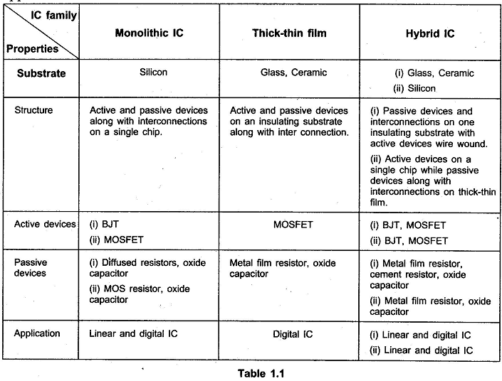
Depending upon the functional utility, the Integrated Circuits Classification are classified as linear ICs and digital ICs. From the point of view of structural considerations, ICs can be divided as monolithic ICs, thick-thin film ICs and hybrid ICs. The monolithic ICs are most common type of IC. In the monolithic ICs, all the active and passive components along with their interconnections are manufactured on a single silicon chip. In general, the monolithic ICs has power limitations ; hence they are preferred only in low power applications.
For slightly higher power applications, the thick-thin film ICs are employed. These are larger in size than the monolithic ICs; but smaller in size than the discrete circuits. With thick-thin film ICs, some of the passive components like resistors, capacitors are integrated, but the components like BJT, diodes are connected as discrete components to complete the circuit. Thus,.in general, thick-thin film circuits are the combinations of integrated and discrete components.
For high power applications, hybrid ICs are used. Hybrid ICs combine two or more monolithic ICs in one package. They may combine monolithic ICs with thick-thin film circuits.
On the basis of the active devices used, the ICs are classified as bipolar ICs and unipolar ICs. The bipolar ICs use bipolar junction transistors (BJTs), while the unipolar ICs use field effect transistors (FETs).
Depending upon the isolation technique used, the bipolar ICs are further classified as p-n junction isolation ICs and dielectric isolation ICs.
Depending upon the type of FET used, the unipolar ICs are further classified as MOSFET unipolar ICs and JFET unipolar ICs.
Table 1.1 gives the total information about the IC families on the basis of substrate used, structure of IC, active and passive devices used and finally the application of the IC. °
Integrated Circuit Chip Size and Levels of Integration:
In 1947, Prof. Bardeen and Prof. Brattain, the members of a research group at Bell Laboratories, invented first germanium transistor. Actually the team was attempting to make a device resembling a field effect transistor. Even though the basic principle behind the operation of MOSFET was proposed in 1935, it took long ‘period to materialize this device. By the year of 1951, the bipolar junction transistors (BJTs) and the junction field effect transistors (JFETs) came in the market. Immediately in 1954, silicon took the place of germanium in BJTs. In late 1960, first time MOSFET was produced.
Meanwhile the interconnection of electric circuits with the help of the printed circuit assembly was under progress. In 1952, the scientist found the possibility of semiconductor Integrated Circuits Classification. Finally in 1958 Jack Kilby of Texas Instruments invented first integrated circuit. Shortly after this invention Prof. Robert Noyce and Gorden Moore of Fairchild semiconductor, USA, announced the planar process for silicon bipolar transistors which stepped ahead to the development of monolithic IC. After realizing the strength of the IC, it become the most demanded device. Then progressively inventions were made in increasing the number of active devices per chip by reducing device dimensions.
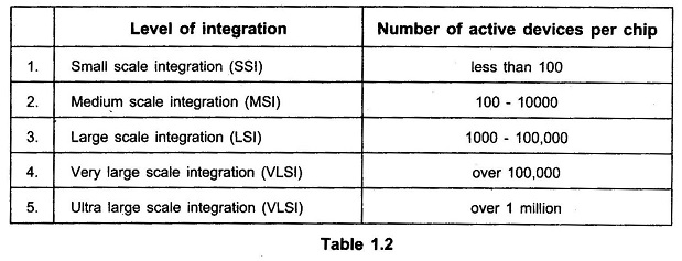
Depending upon the number of active devices per chip, there are different levels of integration as explained below.
When the active devices per chip are less than 100, then it is referred as small scale integration (SSI). Most of the SSI chips use integrated resistors, diodes and bipolar transistors.
When the count of active devices per chip is between 100 to 1000, then it is referred as medium scale integration (MSI). In most of the MSI chips, BJTs and enhancement mode MOSFETs are integrated.
In large scale integration (LSI) ICs, the number of active devices per chip ranges between 1000 to 100,000. In general, LSI chips use MOS transistors; as it requires less number of steps for integration. Thus more number of components can be produced on the chip with MOS transistors than with the bipolar transistors.
When the active devices per chip are over hundreds of thousands, then it is referred as very large scale integration (VLSI). Almost all modern chips employ VLSI technique.
Recently a new level of integration has been introduced which is known as ultra large scale integration (ULSI). In ULSI technique, more than one million active devices are integrated on a single chip. Pentium microprocessors use ULSI technology.
Table 1.2 gives the categories of ICs on the basis of number of active devices. Note that the number of active devices per chip is nothing but the number of transistors per chip. Sometimes an alternative parameter for transistor count per chip may be used. It is referred as gate count.
Monolithic IC Technology Fundamentals:
We have already studied that in monolithic ICs all the active as well as passive components along with interconnections are integrated on a single crystal. The word ‘monolithic’ is originated from Greek word and means ‘single stone’ or ‘one stone’. Thus this word is appropriate as the components are integrated on a single piece of silicon crystal. The fabrication of different discrete devices such as diodes, transistors and Integrated Circuits Classification is carried out by the same technology. The various processes involved in the fabrication of different devices are carried out in a single plane. Hence this is also referred as a planar technology.

