Interfacing ICs Articles:
Features of 8255 Microprocessor: Here we see programmable peripheral interface (PPI), 8255, designed by Intel. It is a general purpose programmable I/O device used for parallel data transfer. It has 24 I/O pins which can be … (Read More)
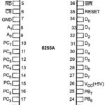
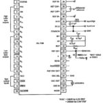
8255 Pin Diagram: Fig. 14.1 shows the 8255 Pin Diagram of Microprocessor. 8255 Block Diagram: Fig. 14.2 shows the internal 8255 block diagram of 8255 Pin Diagram Microprocessor. It consists of data bus buffer, control logic and Group A and Group B controls. Data … (Read More)
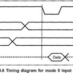
8255 Programming and Operation: The 8255 Programming and Operation are follows Programming in Mode 0: The Ports A, B and C can be configured as simple input or output ports by writing the appropriate control word in the control word register. In the control … (Read More)
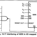
8255 Interfacing with 8086: Fig. 14.17 shows the 8255 Interfacing with 8086 Microprocessor and Interfacing 8255 with 8085 Microprocessor in I/O mapped I/O technique. Here RD and WR signals are activated when IO/M signal is high, indicating I/O bus cycle. Reset … (Read More)
Serial Communication Interface 8251: Most of the microprocessors are designed for parallel communication. In parallel communication number of lines required to transfer data depend on the number of bits to be transferred. For example, to transfer a byte of data, 8 … (Read More)
Features of 8251 Microcontroller: The features of Features of 8251 Microcontroller are namely, 1. The Intel 8251A is an universal synchronous and asynchronous communication controller. 2. It supports standard asynchronous protocol with : 5 to 8 Bit character format odd, even or no parity generation and … (Read More)
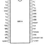
8251 Pin Diagram: Fig. 14.36 shows the 8251 Pin Diagram. Data Bus : Bi-directional, tri-state, 8-bit Data Bus. This pin allow transfer of bytes between the CPU and the 8251A. RD (Read) : A low on this input allows the CPU to read … (Read More)
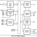
8251 Block Diagram in Microprocessor: Fig. 14.37 shows the 8251 Block Diagram in Microprocessor. It includes : Data bus buffer, Read/Write control logic, modem control, Transmit buffer, Transmit Control, Receiver Buffer and Receiver control. Data Bus Buffer : This tri-state, bi-directional, 8-bit … (Read More)
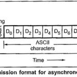
 8251 Usart: We know that, 8251A is Universal Synchronous, Asynchronous, Receiver, and Transmitter. Therefore 8251 Usart can take place with four different ways. Asynchronous transmission Asynchronous reception Synchronous transmission Synchronous reception These communication modes can be enabled by writing proper mode and command … (Read More)
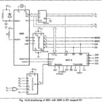
Interfacing 8251 with 8085: Fig. 14.44 shows the Interfacing 8251 with 8085 in I/O mapped I/O technique. Here, RD and WR signals are activated by CPU when IO/M signal is high, indicating I/O bus cycle. The address line A0 is connected to … (Read More)
8257 DMA Controller: In microprocessor based systems data transfer can be controlled by either software or hardware. Upto this point we have used program instructions to transfer data from I/O device to memory or from memory to I/O device. To transfer … (Read More)
Features of Microprocessor 8257 DMA Controller: The Features of Microprocessor 8257 DMA Controller are follows, 1. It is a programmable; 4-channel, direct memory access controller. Each channel can be programmed individually. Therefore, we can interface 4 input/output devices with 8257. 2. Each channel … (Read More)
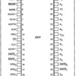
8257 Pin Diagram: Fig. 14.61 shows 8257 Pin Diagram. Data Bus (D0-D7) : These are bi-directional tri-state signals connected to the system data bus. When CPU is having control of system bus it can access contents of address register, status register, mode … (Read More)
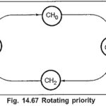
Operating Modes of 8257: The Operating Modes of 8257 can be programmed to operate in following modes : Rotating Priority Mode : In rotating priority mode, the priority of the channels has a circular sequence. In this, channel being serviced gets the lowest … (Read More)
Interfacing of 8257 with 8085: Fig. 14.68 shows the interfacing of 8257 with 8085 in I/O mapped I/O technique. In slave mode, RD and WR signals are activated by CPU when IO/M signal is high, indicating I/O bus cycle. In master … (Read More)
Features of 8259 Programmable Interrupt Controller: The Features of 8259 Programmable Interrupt Controller are 1. It can manage eight priority interrupts. This is equivalent to providing eight interrupt pins on the processor in place of INTR pin. 2. It is possible to locate vector … (Read More)
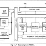
8259 Block Diagram: Fig. 14.71 shows the internal 8259 Block Diagram. It includes eight blocks : data bus buffer, read/write logic, control logic, three registers (IRR, ISR and IMR), priority resolver, and cascade buffer. Data Bus Buffer: The data bus buffer allows the … (Read More)
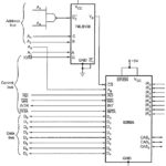
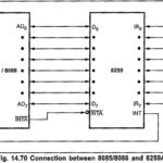
Interfacing 8259 with 8085: Fig. 14.72 shows Interfacing 8259 with 8085 microprocessor system. Addressing of 8259A : The 74LS138 address decoder will assert the CS input of the 8259A when an I/O base address is F0H or F1H on the address bus. The … (Read More)
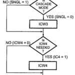
8259 Programmable Interrupt Controller: The 8259 Programmable Interrupt Controller requires two types of command words. Initialization Command Words (ICWs) and Operational Command Words (OCWs). The 8259 Programmable Interrupt Controller can be initialized with four ICWs; the first two are compulsory, and … (Read More)
Features of Intel 8279 Programmable Keyboard Display Interface: The Intel 8279 is a general purpose programmable keyboard and display I/O interface device designed for use with Intel microprocessors. The Features of Intel 8279 Programmable Keyboard Display Interface are 1. It provides a … (Read More)
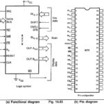
Pin Diagram of 8279: Fig. 14.83 shows functional and pin diagram of 8279. It is a 40 pin device and looking at Fig. 14.83 (a) we can see that these pins are divided in four functional groups : CPU interface Key data Display data Scan CPU … (Read More)
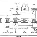
8279 Block Diagram: Fig. 14.84 shows the 8279 Block Diagram. It consists of four main sections CPU interface and control section Scan section 8279 Keyboard section Display section 1.CPU Interface and Control Section: This section consists of data buffers, I/O control, control and timing registers, and timing … (Read More)
Operating Modes of 8279: The Operating Modes of 8279 provides 3 basic input modes : Scanned keyboard Scanned sensor matrix Strobed input Scanned Keyboard: In this mode, keyboard can be scaned in two ways : Encoded scan and decoded scan. Encoded scan : In the encoded scan, … (Read More)
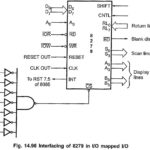
8279 Keyboard Display Controller Interfacing with 8085: Fig. 14.98 shows the 8279 Keyboard Display Controller Interfacing with 8085 in I/O mapped I/O technique. Here RD and WR signals are activated when IO/M signal is high, indicating I/O bus cycle. Reset out … (Read More)
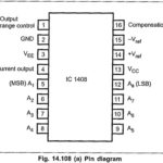
IC 1408 DAC Pin Diagram: The IC 1408 DAC Pin Diagram is an 8 bit R/2R ladder type D/A converter compatible with TTL and CMOS logic. It is designed to use where the output current is linear product of an eight … (Read More)
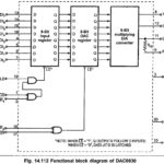
DAC0830 Digital to Analog Converter: The DAC0830 Digital to Analog Converter is an advanced CMOS 8-bit DAC designed to interface directly with the 8080, 8048, 8085, Z80, and other popular microprocessors. A deposited silicon-chromium R-2R resistor ladder network divides. the reference … (Read More)
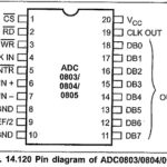
ADC0804 Family: The ADC0804 Family are ADC0803, ADC0804 and ADC0805 are CMOS 8-bit successive-approximation analog to digital converters. These devices are design to operate from common microprocessor control buses, with tri-state output latches driving the data bus, and are identical except … (Read More)
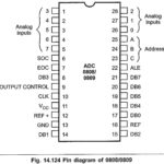
ADC0808 Pin Diagram: The ADC0808 Pin Diagram and ADC 0809 are monolithic CMOS devices with an 8-channel multiplexer. These devices are also designed to operate from common microprocessor control buses, with tri-state output latches driving the data bus. The main features of … (Read More)
IC 7109 Features: The IC 7109 Features are namely, IC 7109 is a 12-bit dual slope A/D converter. It has polarity and overrange bits. It has byte organized TTL compatible three-state outputs and UART handshake mode for simple parallel or serial interfacing to microprocessor … (Read More)
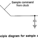
Sample and Hold IC: For accurate analog to digital conversion the analog input voltage should be held constant during the conversion cycle. If the analog input voltage changes by more than ± 1/2 LSB an error … (Read More)
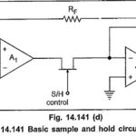
Sample and Hold Circuit: Four basic sample and hold circuit are shown in Fig. 14.141. In these circuits a JFET is used as switch. During the sampling time the JFET switch is turned on, and the holding capacitor charges up to … (Read More)