Lithography Process in IC Fabrication:
Lithography Process is used to produce a multiple image on the resists which covers the wafer. A Lithography Process in IC Fabrication can be realised with the help of three sub processes given by,
- Deposit of the resist,
- Imaging of the wafer, and
- Etching of the oxide.
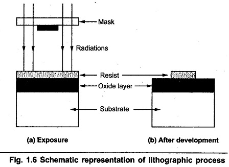
In Lithography Process, the radiation from a source is directed towards the mask on which circuit pattern is present. Some of the radiation transmit through the clear or transparent portion of the circuit. While the opaque portion blocks the radiation. The schematic of the Lithography Process in IC Fabrication is as shown in the Fig. 1.6.
The source used for generating radiation may be ultra violet light (UV), electrons, x-rays and ions. Out of these sources, the most commonly used source is an ultra-violet light source. The process using UV light source is called optical lithography.
Optical Lithography:
In optical lithography, the images are formed with the help of visible or ultra violet rays using contact printing, proximity printing or projection printing.
Two types of Optical Lithography Process:
- Making of photographic mask
- Photoetching
First of all in making of mask, the initial layout is prepared. Then this layout is decomposed into several layers which are called mask layers. The peculiarity of these layers is that each layer corresponds to the process step in the IC fabrication such as base diffusion mask layer, collector diffusion mask layer, metallization mask layer etc.
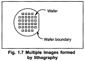
The function of Lithography Process in IC Fabrication is to produce a multiple image on the resist and the wafer as shown in the Fig. 1.7.
The mask for each level consists a multiple image pattern with exactly identical boundaries but different patterns.
The imaging source is either a mask or reticle made up of a glass plate with patterned chromium. The main difference between the mask and the reticle is that there are multiple images with actual size on the mask, while a single enlarged image on a reticle. The mask and reticle are produced with e-beam optical method. Firstly the resist is deposited on a glass plate. Then it is exposed to imaging pattern. After exposure the selective part is removed. Finally etching process is employed to obtain patterned chromium layer on the glass.
After preparing mask for each layer, individual mask is photographed. Then using step and repeat camera, the photo repeating is done. The photographic plate is placed on a mavable platform. During exposure the plate is moved in equal steps such that successive images are formed in array. After developing the exposed plate, master mask is prepared. Generally, the master masks are prepared using contact printing mechanism.
Photo Etching Process:
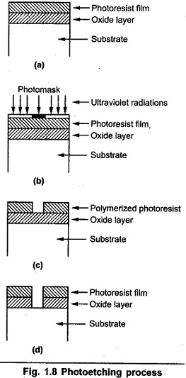
The photo etching is a process of removing SiO2 from the selective regions so that the desired impurities are diffused. The silicon wafer is coated with a photoresist film as shown in the Fig. 1.8 (a).
There are two types of the Photo Resists:
- A Negative Photoresist is the one which becomes less soluble in developer when exposed to light.
- While the Positive Photoresist becomes more soluble when exposed to light.
The examples of negative and positive photo resists are Kodak microneg 747 and MP-2400, HPR-206 respectively.
After coating a wafer with photoresist, the prepared mask is placed over the photoresist coated silicon wafer as shown in the Fig. 1.8 (b). Then it is exposed to UV light. This polymerizes the photoresist present below mask. After removing mask, the wafer is developed using trichloroethylene. Because of the chemical reaction, the unpolymerized and unexposed regions on the photoresist dissolve. The last step in photoetching is to clean the polymerized photoresist. Then the wafer is dipped in etchant solution such as hydrofluoric acid. The silicon dioxide is removed by etching from the areas which are not covered by a photoresist.


