LM340 Series Voltage Regulator:
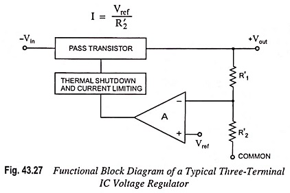
This LM340 Series Voltage Regulator is typical of the three-terminal voltage regulators. The block diagram is shown in Fig. 43.27. The built-in reference voltage Vref drives the noninverting input of an op-amp. The operational amplifier consists of several stages of voltage gain. Because of the high gain of the op-amp, the error voltage between the two input terminals of the op-amp approaches zero. So the inverting input voltage is approximately equal to Vref. This means that current flowing through the potential divider is
Incidentally, the prime attached to R′2 indicates that this resistor is inside the IC itself, rather than being an external resistor. Since the same current flows through R′1, the output voltage is given as
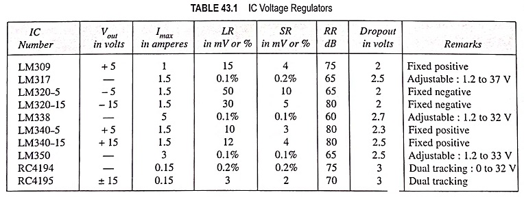
Thus the output voltage of the regulator can be precisely controlled by setting up the desired values of R′1 and R′2. The data for LM 340-5 and LM 340-15 are given in Table 43.1.
The chip includes a pass transistor that can handle more than 1.5 A of load current provided that adequate heat sinking is used. Also included are thermal shutdown and current limiting. Thermal shutdown means that the chip will automatically turn itself off if the internal temperature becomes excessive, around 175°C. This is a precaution against excessive power dissipation, that depends on the ambient temperature, type of heat sinking, and other variables. Because of thermal shutdown and current limiting, devices in the LM340 Series Voltage Regulator are almost indestructible.
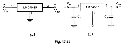
Figure 43.28 (a) shows an LM 340-15 connected as a fixed voltage regulator, pin 1 is the input, pin 3 is the output, and pin 2 is ground.
When an IC is more than a few cm from the filter capacitor of the unregulated power supply, the lead inductance may give rise to oscillations within the IC, Capacitor C1 is required on pin 1 because of only this reason. Capacitor C2 is sometimes used to improve the transient response of the circuit. Refer to Fig. 43.28 (b).
Any device in the LM340 Series Voltage Regulator needs a minimum input voltage at least 2 to 3 V greater than the regulated output voltage. Otherwise, it will stop regulating. Further more, there is a maximum input voltage because of excessive power dissipation.


