Multicavity Klystron:
The design of the multicavity klystron, together with all the remaining tubes described here, relies on the fact that transit time will sooner or later terminate the usefulness of any orthodox tube. They therefore use the transit time, instead of fighting it. The Multicavity Klystron was invented just before World War II by the Varian brothers as a source and amplifier of microwaves. It provided much higher powers than had previously been obtainable at these frequencies.
Operation of Two Cavity Klystron Amplifier:
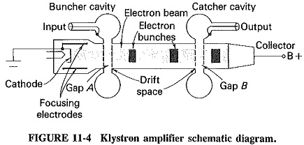
Figure 11-4 schematically shows the principal features of a Two Cavity Klystron Amplifier. It is seen that a high-velocity electron beam is formed, focused (external magnetic focusing is omitted for simplicity) and sent down a long glass tube to a collector electrode which is at a high positive potential with respect to the cathode. The beam passes gap A in the buncher cavity, to which the RF signal to be amplified is applied, and it is then allowed to drift freely, without any influence from RF fields, until it reaches gap B in the output or catcher cavity. If all goes well, oscillations will be excited in the second cavity which are of a power much higher than those in the buncher cavity, so that a large output can be achieved. The beam is then collected by the collector electrode.
The cavities are reentrant and are also tunable (although this is not shown). They may be integral or demountable. In the latter case, the wire grid meshes are connected to rings external to the glass envelope, and cavities may be attached to the rings. The drift space is quite long, and the transit time in it is put to use. The gaps must be short so that the voltage across them does not change significantly during the passage of a particular bunch of electrons; having a high collector voltage helps in this regard.
It is apparent that the electron beam, which has a constant velocity as it approaches gap A, will be affected by the presence of an RF voltage across the gap, as was outlined. The extent of this effect on any one electron will depend on the voltage across the gap when the electron passes this gap. It is thus necessary to investigate the effect of the gap voltage upon individual electrons.
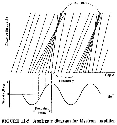
Consider the situation when there is no voltage across the gap. Electrons passing it are unaffected and continue on the collector with the same constant velocities they had before approaching the gap (this is shown at the left of Figure 11-5). After an input has been fed to the buncher cavity, an electron will pass gap A at the time when the voltage across this gap is zero and going positive. Let this be the reference electron y. It is of course unaffected by the gap, and thus it is shown with the same slope on the Applegate diagram of Figure 11-5 as electrons passing the gap before any signal was applied.
Another electron, z, passes gap A slightly later than y. Had there been no gap voltage, both electrons would have continued past the gap with unchanged velocity, and therefore neither could have caught up with the other. Here, electron z is slightly accelerated by the now positive voltage across gap A, and given enough time, it will catch up with the reference electron. As shown in Figure 11-5, it has enough time to catch electron y easily before gap B is approached. Electron x passes gap A slightly before the reference electron. Although it passed gap A before electron y, it was retarded somewhat by the negative voltage then present across the gap. Since electron y was not so retarded, it has an excellent chance of catching electron x before gap B (this it does, as shown in Figure 11-5).
As electrons pass the buncher gap, they are velocity-modulated by the RF voltage existing across this gap. Such velocity modulation would not be sufficient, in itself, to allow amplification by the Multicavity Klystron. Electrons have the opportunity of catching up with other electrons in the drift space. When an electron catches up with another one, it may simply pass it and forge ahead. It may exchange energy with the slower electron, giving it some of its excess velocity, and the two bunch together and move on with the average velocity of the beam. As the beam progresses farther down the drift tube, k) the•bunching becomes more complete, as more and more of the faster electrons catch up with bunches ahead. Eventually, the current passes the catcher gap in quite pronounced bunches and therefore varies cyclically with time. This variation in current density is known as current modulation, and this is what enables the Multicavity Klystron to have significant gain.
It will be noted from the Applegate diagram that bunching can occur once per cycle, centering on the reference electron. The limits of bunching are also shown. Electrons arriving slightly after the second limit clearly are not accelerated sufficiently to catch the reference electron, and the reference electron cannot catch any electron passing gap A just before the first limit. Bunches thus also arrive at the catcher gap once per cycle and deliver energy to this cavity. In ordinary vacuum tubes, a little RF power applied to the grid can cause large variations in the anode current, thus controlling large amounts of dc anode power. Similarly in the klystron, a little RF power applied to the buncher cavity results in large beam current pulses being applied to the catcher cavity, with a considerable power gain as the result. Needless to say, the catcher cavity is excited into oscillations at its resonant frequency (which is equal to the input frequency), and a large sinusoidal output can be obtained because of the flywheel effect of the output resonator.
The construction of the Multicavity Klystron lends itself to two practical microwave applications as a multicavity power amplifier or as a two-cavity power oscillator.
Multicavity Klystron Amplifier:
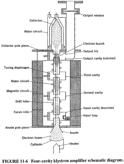
The bunching process in a two-cavity klystron is by no means complete, since there are large numbers of out-of-phase electrons arriving at the catcher cavity between bunches. Consequently, more than two cavities are always employed in practical klystron amplifiers. Four cavities are shown in the klystron amplifier schematic diagram of Figure 11-6 and up to seven cavities have been used in practice. Partially bunched current pulses will now also excite oscillations in the intermediate cavities, and these cavities in turn set up gap voltages which help to produce more complete bunching. Having the extra cavities helps to improve the efficiency and power gain considerably. The cavities may all be tuned to the same frequency, such synchronous tuning being employed for narrowband operation. For broadband work, for example with UHF klystrons used as TV transmitter output tubes, or 6-GHz tubes used as power amplifiers in some satellite station transmitters, stagger tuning is used. Here, the intermediate cavities are tuned to either side of the center frequency, improving the bandwidth very significantly. It should be noted that cavity Q is so high that stagger tithing is a “must” for bandwidths much over 1 percent.
Two Cavity Klystron Oscillator:
If a portion of the signal in the catcher cavity is coupled back to the buncher cavity, oscillations will take place. As with other oscillators, the feedback must have the correct polarity and sufficient amplitude. The schematic diagram of such an oscillator is as shown in Figure 11-4, except for the addition of a (permanent) feedback loop. Oscillations in the two-cavity klystron behave as in any other feedback oscillator. Having been started by a switching transient or noise impulse, they continue as long as dc power is present.
Performance and applications:
The multicavity klystron is used as a medium-, high- and very high-power amplifier in the UHF and microwave ranges, for either continuous or pulsed operation. The frequency range covered is from about 250 MHz to over 95 GHz, and the power available has been described as “adequate,” i.e., much higher then currently needed. Table 11-1 illustrates this situation.
This table summarizes the power requirements of the major applications for klystron amplifiers and shows how the devices are able to meet them. The gain of klystrons is also adequate. It ranges from 30-35 dB at UHF to 60-65 dB in the microwave range. Such high gain figures mean that the klystron is generally the only nonsemiconductor device in high-power amplifiers. For example, the Varian VKX7809 X-band klystron has a CW power output of 2.2 kW with a gain of 46 dB. Hence the driving power required is only 50 mW, which is well within the capability of any semiconductor power device.
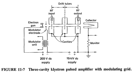
Current klystron developments are aimed at improving efficiency, providing longer lives, and reducing size; typical efficiency is 35 to 50 percent. To improve reliability and MTBF (mean time between failures), tungsten-iridium cathodes are now being used to reduce cathode temperature and thus provide longer life. As regards size, a typical 50-kW UHF klystron, as shown in Figure 11-6, may be over 2 m long, with a weight of nearly 250 kg. As may be gathered from Figure 11-6, a large proportion of the bulk is due to the magnet, often as much as two-thirds. A 100-kW peak (2.5-kW average) X-band klystron may be 50 cm long and may weigh about 30 kg, if it uses permanent-magnet focusing. It is possible to reduce this weight to one-third by using periodic permanent-magnet (PPM) focusing. In this system, the beam is focused by so-called magnetic lenses, which are small, strong magnets along the beam path. In between them, the beam is allowed to defocus a little. The use of grids for modulation purposes (see Figure 11-7) has been rediscovered and evolved further.
The two-cavity klystron oscillator has fallen out of favor, having been displaced by CW magnetrons, semiconductor devices and the high gain of klystron and TWT amplifiers.
Further practical aspects:
Multicavity klystron amplifiers suffer from the noise caused because bunching is never complete, and so electrons arrive at random at the catcher cavity. This makes them too noisy for use in receivers, but their typically 35-dB noise figures are more than adequate for transmitters.
Since the time taken by a given electron bunch to pass through the drift tube of a klystron is obviously influenced by the collector voltage, this voltage must be regulated. Indeed, the power supplies for Multicavity Klystron are quite elaborate, with a regulated 9 kV at 750-mA collector current required for a typical communications klystron. Similarly, when a klystron amplifier is pulsed, such pulses are often applied to the collector. They should be flat, or else frequency drift (within limits imposed by cavity bandwidth) will take place during the pulse. As an alternative to this, and also because collector pulsing takes a lot of power, modulation of a special grid has been developed, as shown in Figure 11-7. Atypical “gain” of 20 is available between this electrode and the collector, thus reducing the modulating power requirements twentyfold. Amplitude modulation of the klystron can also be applied via this grid. However, if amplitude linearity is required, it should be noted that the klystron amplifier begins to saturate at about 70 percent of maximum power output. Beyond this point, output still increases with input but no longer linearly. This saturation is not a significant problem, all in all, because most of the CW applications of the multicavity klystron involve frequency modulation. Under such conditions, e.g., in a troposcatter link, the klystron merely amplifies a signal that is already frequency-modulated and at a constant amplitude.


