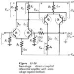
DC Feedback Pair with Two Amplification Stages
DC Feedback Pair with Two Amplification Stages: The DC Feedback Pair with Two Amplification Stages circuit shown in Fig. 12-25(a). The base of transistor Q2 is directly connected to the…
Two Stage Direct Coupled Common Emitter Amplifier: Figure 12-23 shows Two Stage Direct Coupled Common Emitter Amplifier. This time the second stage is a common collector circuit, or emitter follower.…
FET and BJT Difference: FET and BJT Difference (CS, CD, and CG Circuit Comparison) - Table 11-1 compares Zi, Zo and Av for CS, CD, and CG circuits. As already discussed, the…
Common Drain Amplifier Circuit Diagram: The FET Common Drain Amplifier Circuit Diagram shown in Fig. 11-14 has the output voltage developed across the source resistor (RS). The external load (RL)…
High Frequency Analysis of BJT: Coupling and Bypass Capacitor Effects - Consider the typical High Frequency Analysis of BJT illustrated in Fig. 8-5. As discussed, the amplifier voltage gain is…
BJT Cutoff Frequency and Capacitance: Device Cutoff Frequency - All transistors have junction capacitances. The junction capacitances and the transit time of charge carriers through the semiconductor material limit the…
Difference Between Common Base Common Emitter and Common Collector: Table 6-2 compares Zi, Zo, and Av, for difference Between Common Base Common Emitter and Common Collector circuits. As already discussed, the…
Common Collector Circuit Analysis: In the Common Collector Circuit Analysis (CC) shown in Fig. 6-28 the external load (RL) is capacitor-coupled to the transistor emitter terminal. The circuit uses voltage divider…