FET and BJT Difference
FET and BJT Difference: FET and BJT Difference (CS, CD, and CG Circuit Comparison) - Table 11-1 compares Zi, Zo and Av for CS, CD, and CG circuits. As already discussed, the…
Continue Reading
FET and BJT Difference
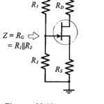
FET and BJT Difference: FET and BJT Difference (CS, CD, and CG Circuit Comparison) - Table 11-1 compares Zi, Zo and Av for CS, CD, and CG circuits. As already discussed, the…
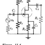
Common Source Circuit Analysis: A FET Common Source Circuit Analysis is shown in Fig. 11-6. With the capacitors treated as ac short-circuits, the circuit input terminals are the gate and…
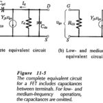
FET Equivalent Circuit Model: The complete FET Equivalent Circuit Model is shown in Fig. 11-5(a). It is seen that tilt source terminal is common to both input and out, so…
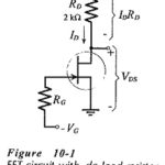
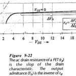
DC Load Line for FET: The DC Load Line for FET circuit is drawn on the device output characteristics (or drain characteristics) in exactly the same way as for a…
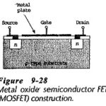
MOSFET Construction and Characteristics: Figure 9-28 shows the MOSFET Construction and Characteristics of a metal oxide semiconductor FET (MOSFET), also known as an insulated gate FET. Starting with a high-resistive…
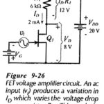
FET Amplification: Consider the n-channel FET Amplification circuit in Fig. 9-26. Note that drain-source terminals are provided with a dc supply (VDD), connected via the drain resistor (R1). The gate-source…
FET Datasheet Specifications: Maximum Ratings - A portion of a FET Datasheet Specifications is reproduced in Fig. 9-17. As with other device data sheets, a device type number and brief description is…
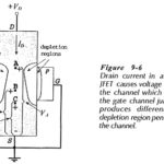
JFET Characteristics: An n-channel JFET Characteristics block representation is shown in Fig. 9-6. With a drain-source voltage applied as illustrated, ID flows in the direction shown producing voltage drops along…