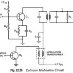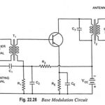
Base Modulation Circuit Working Principle
Base Modulation Circuit Working Principle: The circuit for base modulation is shown in Fig. 22.28. The carrier signal from a crystal oscillator is coupled to the base terminal of the…
Continue Reading
Base Modulation Circuit Working Principle