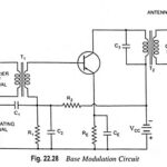
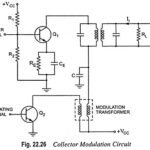
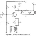
Emitter Modulation – Circuit Diagram and its Operation
Emitter Modulation - Circuit Diagram and its Operation: The circuit for emitter modulation is shown in Fig. 22.29. It is essentially a CE amplifier. The carrier signal from a crystal…
Base Modulation Circuit Working Principle: The circuit for base modulation is shown in Fig. 22.28. The carrier signal from a crystal oscillator is coupled to the base terminal of the…
Collector Modulation Circuit - Working, Advantages and Disadvantages: This is very popular method for AM generation. The circuit diagram for collector modulation is shown in Fig. 22.26. Here, the transistor…
Emitter Follower Circuit - Operation, Advantages and Applications: Emitter Follower Circuit is also a negative current feedback circuit. This circuits exhibits a large input impedance, a small output impedance, and…
What is Crossover Distortion and how to eliminate it? In addition to the distortion introduced due to the nonlinearity of the collector characteristics and due to non-matching of the two…
What is Low Frequency Compensation? The coupling or blocking capacitor tilts the amplifier response for step input. In Fig. 16.28, if a high value of resistance Rd is added in…
Depletion Type MOSFET - Construction, Operation and Characteristics: As we know already that when the gate is biased negative w.r.t. the source in an N-channel JFET, the depletion-region widths are…
Metal Insulator Semiconductor Field Effect Transistors (MISFETs): The Metal Insulator Semiconductor Field Effect Transistors (MISFETs) is one of the most widely used electronic devices, particularly in digital circuits, because of…