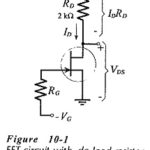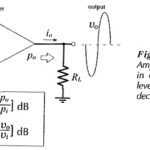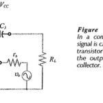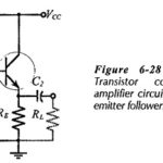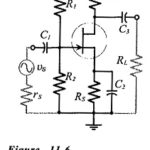
Common Source Circuit Analysis
Common Source Circuit Analysis: A FET Common Source Circuit Analysis is shown in Fig. 11-6. With the capacitors treated as ac short-circuits, the circuit input terminals are the gate and…
Continue Reading
Common Source Circuit Analysis