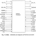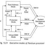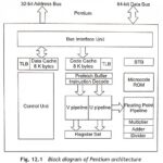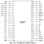
Pin Diagram of 8087 Processor
Pin Diagram of 8087 Processor: Figure 7.46 shows the pin diagram of 8087 processor. The operations of all pins of 8087 are explained below: AD15-AD0 The AD15-AD0 are the time multiplexed address/data…
Continue Reading
Pin Diagram of 8087 Processor