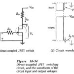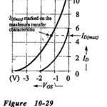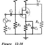
Single Stage Common Source Amplifier
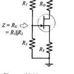
Single Stage Common Source Amplifier: Bias circuit design for the Single Stage Common Source Amplifier in shown in Fig. 12-10. As with the common-emitter BJT circuit, design commences with specification…
Continue Reading
Single Stage Common Source Amplifier