Photoconductive Cell Construction and Working:
Photoconductive Cell Construction and Working – Light striking the surface of a material can provide sufficient energy to cause electrons within the material to break away from their atoms. Thus, free electrons and holes (charge carriers) are created within the material, and consequently its resistance is reduced. This is known as the Photoconductive effect.
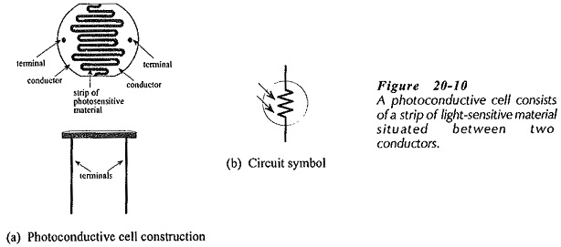
The Photoconductive Cell Construction and Working is illustrated in Fig. 20-10(a), and the graphic symbol is shown in Fig. 20-10(b). Light-sensitive material is arranged in the form of a long strip zigzagged across a disc-shaped base. The connecting terminals are fitted to the conducting material on each side of the strip; they are not at the ends of the strip. Thus, the light sensitive material is actually a short, wide strip between the two conductors. For added protection, a transparent plastic cover is usually included.
Cadmium sulfide (CdS) and cadmium selenide (CdSe) are the two materials normally used in photoconductive cell manufacture. Both respond rather slowly to changes in light intensity. For cadmium selenide, the response time (tres) is around 10 ms, while for cadmium sulfide it may be as long as 100 ms. Temperature sensitivity is another important difference between the two materials There is a large change in the resistance of a cadmium selenide cell with changes in ambient temperature, but the resistance of cadmium sulfide remains relatively stable. As with all other devices, care must be taken to ensure that the power dissipation is not excessive. The spectral response of a cadmium sulfide cell is similar to that of the human eye; it responds to visible light. For a cadmium selenide cell, the spectral response is at the longer wavelength end of the visible spectrum and extends into the infrared region.
Characteristics and Parameters:
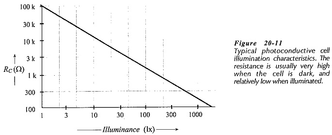
Typical illumination characteristic for a photoccnductive cell are shown in Fig. 20-11. It is seen that, when the cell is not illuminated its resistance can be greater than 100 kΩ. This is known as the dark resistance of the cell. When the cell is illuminated, its resistance might fall to a few hundred ohms. Note that the scales on the illumination characteristic are logarithmic.
A typical photoconductive cell specification is shown in Fig. 20-12. As well as maximum voltage and power dissipation, the cell dark resistance and the resistance at a 10 lx illumination is listed. Note the wide range of cell resistance at a 10 lx. The light wavelength that gives peak response (λP) is also given on the specification. Cell sensitivity is sometimes used, and this is simply the cell current for a given voltage and given level of illumination.
Applications:
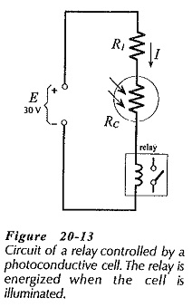
Figure 20-13 shows a photoconductive cell used for relay control. When the cell is illuminated, its resistance is low and the relay current is at its maximum. Thus, the relay is energized. When the cell is dark, its high resistance keeps the current down to a level too low to energize the relay. Resistance R1 is included to limit the relay current to the desired level when the cell resistance is low.
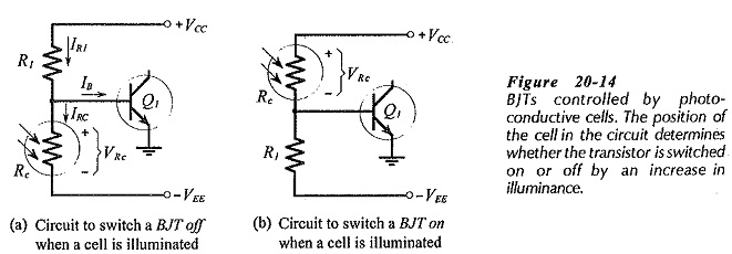
Photoconductive Cell Construction and Working employed to switch transistors on and off are shown in Fig. 20-14. When cell in Fig. 20-14(a) is dark, the cell resistance (RC) is high. Consequently, the transistor base is biased above its emitter voltage level, and Q1 is turned on. When the cell is illuminated, its resistance is reduced, and the lower cell resistance in series with R1 biases the transistor base below its emitter voltage level. Thus Q1 is turned off when the cell is illuminated.
In Fig. 20-14(b), Q1 is biased off when the cell is dark, because RC is high. When illuminated, the reduced cell resistance causes Q1 to be biased on.
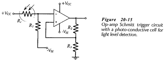
Figure 20-15 shows a photoconductive cell used with an op-amp Schmitt trigger circuit. When the cell resistance is low (cell illuminated), the voltage across R1 is higher than the upper trigger point (UTP) for the Schmitt. Consequently, the op-amp output is tow (negative). The output switches to a high (positive) level when VR1 falls to the Schmitt circuit lower trigger point (LTP). This occurs when the cell illumination level falls, causing RC to rise.
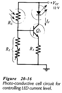
The circuit in Fig. 20-16 uses a photoconductive cell to control the current level in an LED. The LED current is low when the ambient light level is low, because the cell resistance is high. The LED current is increased as a result of the decreased resistance of RC when the ambient light level is high. This increased current gives greater LED brightness so that it can be easily seen.
