Practical Op Amp Characteristics:
The Practical Op Amp Characteristics can be approximated closely enough, for many practical op-amps But basically the Practical Op Amp Characteristics are little bit different than the ideal op-amp characteristics.
The various characteristics of a practical op-amp can be described as below
Open loop gain : It is the voltage gain of the op-amp when no feedback is applied. Practically it is several thousands.
Input impedance : It is finite and typically greater than 1 M Ω. But using FETs for the input stage, it can be increased up to several hundred M Ω.
Output impedance : It is typically few hundred ohms. With the help of negative feedback, it can be reduced to a very small value like 1 or 2 ohms.
Bandwidth : The bandwidth of practical op-amp in open loop configuration is very small. By application of negative feedback, it can be increased to a desired value.
Input offset voltage : Whenever both the input terminals of the op-amp are grounded, ideally, the output voltage should be zero. However, in this condition, the practical op-amp shows a small non zero output voltage. To make this output voltage zero, a small voltage in millivolts is required to be applied to one of the input terminals. Such a voltage makes the output exactly zero. This d.c. voltage, which makes the output voltage zero, when the other terminal is grounded is called input offset voltage denoted as Vios. How much voltage, to which terminal and with what polarity, to be applied, is specified by the manufacturer in the datasheet. The input offset voltage depends on the temperature.
Input bias current : For ideal op-amp, no current flows into the input terminals. The practical op-amps do have some input currents which are very small, of the order of 10– 6 A to 10-14 A.
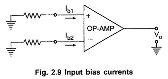
Most of the op-amps use differential amplifier as the input stage. The two transistors of the differential amplifier must be biased correctly. But practically, it is not possible to get exact matching of the two transistors. Thus, the input terminals which are the base terminals of the two transistors, do conduct the small d.c. current. These small base currents of the two transistors are nothing but bias currents denoted as Ib1 and Ib2.
So input bias current can be defined as the current flowing into each of the two input terminals when they are biased to the same voltage level i.e. when the op-amp is balanced.
The two input currents, when op-amp is balanced, are shown in the Fig. 2.9. The two bias currents are never same hence the manufacturers specify the average input bias current Ib, which is found by adding the magnitudes of Ib1 and Ib2 and dividing the sum by 2.
Mathematically it is expressed as,![]() Input offset current : The difference in magnitudes of Ib1 and Ib2 is called as input offset current and is denoted as Iios. Thus,
Input offset current : The difference in magnitudes of Ib1 and Ib2 is called as input offset current and is denoted as Iios. Thus,
Input offset current
![]()
The magnitude of this current is very small, of the order of 20 to 60 nA. It is measured under the condition that input voltage to op-amp is zero.
If we supply equal d.c. currents to the two inputs, output voltage of op-amp must be zero. But practically, there exists some voltage at the output. To make it zero, the two input currents are made to differ by small amount. This difference is nothing but the input offset current.