Quantitative Theory of PN Junction Diode:
Quantitative Theory of PN Junction Diode – Here an expression for the total current will be derived as a function of the applied voltage with the assumption that depletion layer thickness is negligible (i.e., barrier width is zero).
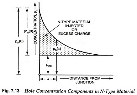
When a P-N diode is forward biased, holes are injected from P-region into the N-region. The concentration pn of the holes in the N-region is increased above its thermal equilibrium value pno. The hole concentration in N-region is given as
where pno is the hole concentration in thermal-equilibrium condition, Lh is the diffusion length for holes in N-type material and x is the distance from the junction where concentration is considered.
The injected, or excess, concentration of holes at x = (0), p′n(0) is given as
These several hole concentration components are shown in Fig. 7.13, which shows that the concentration pn(x) falls exponentially with distance x into the N-type material.
The diffusion hole current in the N-region is given as
Taking the derivative of Eq. (7.4) and substituting the value of dpn/dx in above Eq. (7.6), we have
At junction i.e., x = 0
where A is area of material in m2, Dh is diffusion constant for holes in m2/s, e is the magnitude of charge on holes, Lh is the diffusion length of holes in N-type material in metre, and p′n(0) is the excess of hole concentration at Quantitative Theory of PN Junction Diode.
Using Boltzmann relationship of kinetic theory of gases, we have
where V is the voltage applied across the P-N diode and VT is the volt-equivalent of temperature and it is given as
The Eq. (7.9) is known as the law of junction.
Diffusion Length:
Diffusion length is defined as the distance travelled by free charge carriers (electrons or holes) before recombination. It may also be defined as the average distance covered by an excess charge carrier during its lifetime τ.
The diffusion length Lh and lifetime τh are related to each other as :
Similarly in case of P type semiconductor
Forward Currents:
The total diode current I at x = 0 is given as
where Ihn (0) is the current caused by holes entering the N-region and Iep (0) is the current caused by electrons entering the P-region.
From Eqs. (7.8) and (7.9)
Similarly,
From Eqs. (7.12), (7.13) and (7.14) we have total diode current
where
Reverse Saturation Current:
In the foregoing discussion a positive value of V indicates a forward bias. Equation (7.15) is equally valid for reverse bias [i.e., for negative values of applied voltage V]. For a reverse bias voltage exceeding VT (i.e., 26 mV) at room temperature (27 °C or 300 K), current I → – I0. Thus I0 is called the reverse saturation current.
The concentration of holes in N-type region,
The concentration of electrons in P-type region,
where ND and NA are the concentrations of donor and acceptor atoms respectively.
Substituting pno = n2i/ND and npo = n2i/NA in Eq. (7.16), we have
where VGO is a voltage numerically equal to the forbidden energy gap, EGO in electron volts, and VT is the volt equivalent of temperature and is equal to T/11,600.
For germanium the diffusion constants Dh and De vary approximately inversely proportional to temperature T. Hence I0 may be given as
where K1 is a constant, independent of temperature T.
In the discussion made above, the effect of carrier generation and recombination in the space-charge region has been ignored. Such an assumption is valid for a germanium diode (not for a silicon diode). For the silicon diode, a diffusion current is negligible in comparison with the transition-layer charge-generation current, which is given approximately by
where η ≈ 2 for small (rated) currents and η ≈ 1 for large currents.
Also I0 is found to be proportional to ni instead of n2i so
where K2 is a constant, independent of temperature T.


