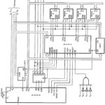
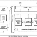
8259 Block Diagram
8259 Block Diagram: Fig. 14.71 shows the internal 8259 Block Diagram. It includes eight blocks : data bus buffer, read/write logic, control logic, three registers (IRR, ISR and IMR), priority…
Interfacing of 8257 with 8085: Fig. 14.68 shows the interfacing of 8257 with 8085 in I/O mapped I/O technique. In slave mode, RD and WR signals are activated by CPU…
8257 Pin Diagram: Fig. 14.61 shows 8257 Pin Diagram. Data Bus (D0-D7) : These are bi-directional tri-state signals connected to the system data bus. When CPU is having control of…
Maximum Mode Configuration of 8086: A processor is in the Maximum Mode Configuration of 8086 when its MN/MX pin is grounded. The maximum mode defines pins 24 to 31 as…
Minimum Mode Configuration of 8086: Pin definitions from 24 to 31 are different for minimum mode and maximum mode. By using these pins the 8086 itself generates all bus control…
Signal Generator in Electronic Instrumentation Articles: What is Signal Generator? A signal generator is a vital component in a test setup, and in electronic troubleshooting and development, whether on a…
High Voltage Test on Circuit Breaker and Isolators: High Voltage Test on Circuit Breaker and Isolators is covered, giving common characteristics for both. While these characteristics are directly relevant to…
8085 Pin Diagram | Functional Pin Diagram of 8085 Microprocessor: Fig. 1.3 (a) and (b) shows 8085 Pin Diagram and functional pin diagram of 8085 microprocessor respectively. The signals of…