Semiconductor Physics Articles:
Elemental Semiconductor Materials: Group IV includes five elements viz., Carbon (C), Silicon (Si), Germanium (Ge), Tin (Sn) and lead (Pb). The elements of this subgroup show marked similarity as well as gradation in properties with rise of atomic number and on … (Read More)
Compound Semiconductor Materials: Most of the compound semiconductor materials are formed from the combinations of group III and group V elements. A portion of the periodic table listing the more common semiconductors is given in Table 6.2. A list of some semiconductor materials … (Read More)
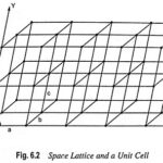
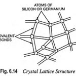
What is Crystalline Structure? Solids are characterized by incompressibility, rigidity and mechanical strength. This indicates that the molecules, atoms or ions that make up a solid are closely packed, i.e., they are held together by strong … (Read More)
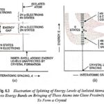
Energy Band Theory of Crystals: As discussed above, it is revealed that most metals and semiconductors are crystalline in structure and a crystal is made up of a space array of atoms or molecules (strictly … (Read More)
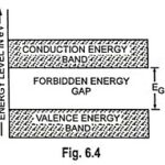
Energy Band Diagram of Semiconductors, Insulators and Metals: Energy Band Diagram of Semiconductors, Insulators and Metals – As discussed earlier, the electrons of an isolated atom are acted upon only by the forces within that atom. However, when atoms are brought … (Read More)
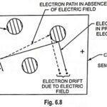
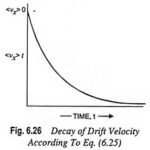
Drift Current and Diffusion Current in Semiconductor: The two basic processes which cause electrons and holes to move in a semiconductor are : drift, which is the movement caused by electric fields, and diffusion, which is the flow caused by variations in the … (Read More)
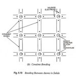
What is Atomic Bonds and Types? Whether a material is a conductor, a semiconductor, or an insulator depends largely upon what happens to the outer-shell electrons when the atoms bond themselves together to form a solid. Atomic bonds arc of two … (Read More)
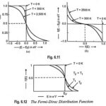
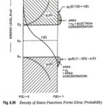
Fermi Dirac Function in Semiconductor: It is important to know what energies are possessed by a mobile carrier in a solid or semiconductor. This relationship is referred to as energy distribution function. We are concerned with the distribution of energy of … (Read More)
What is Intrinsic Semiconductor? An intrinsic semiconductor is one which is made of the semiconductor material in its extremely pure form. A semiconductor is not truly intrinsic unless its impurity content is less than one part in 100 million parts of … (Read More)
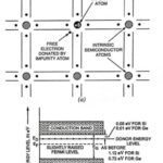
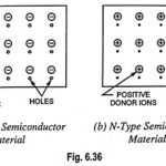
What is Extrinsic Semiconductor? Intrinsic (or pure) semiconductor by itself is of little significance as it has little current conduction capability at ordinary room temperature. However, the electrical conductivity of intrinsic semiconductor can be increased many times by adding very small … (Read More)
Mass Action Law in Semiconductor: As already mentioned, concentration of free electrons and holes is always equal in an intrinsic semiconductor. When N-type impurity is added to an intrinsic semiconductor, the concentration of free electrons is increased (or the concentration of … (Read More)
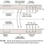
Charge Densities in Extrinsic Semiconductor: Equation (6.19) provides relationship between the electron and hole concentrations n and p respectively. If ND is the concentration of donor atoms, there will be ND immobile positive charges per unit … (Read More)
Relaxation Time, Collision Time and Mean Free Path: The relaxation time is closely related to the mean time of flight between collision and also to the mean free path of the conduction electrons, which is the average distance of undisturbed motion … (Read More)
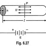
Explain Conductivity of Metals: Consider a conductor of length l metres and cross-sectional area A square metres, as shown in Fig. 6.27. Let the number of free electrons available per m3 of the conductor material i.e., electron … (Read More)
Explain Conduction in Intrinsic Semiconductors: As already explained, conduction through a semiconductor is due to two mechanisms viz. drift and diffusion. The movement of charge carriers (electrons and holes) under the influence of an applied … (Read More)
Carrier Concentration in Intrinsic Semiconductor: For determination of the conductivity of a semiconductor, it is essential to know the Carrier Concentration in Intrinsic Semiconductor of free electrons in conduction band and concentration of holes in valence band. Number of Electrons in the … (Read More)
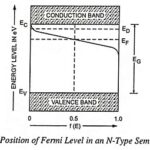
Fermi Level in Extrinsic Semiconductor: The equation for f(E) specifying the fraction of all states at energy E (electron volts) occupied under conditions of thermal equilibrium is called the Fermi-Dirac probability function and is given as where k is Boltzmann constant in … (Read More)
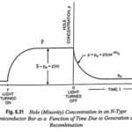
Carrier Lifetime in Semiconductor: As already explained, in an extrinsic semiconductor the number of holes is equal to the number of free electrons. Due to thermal agitation, new electron-hole pairs are continually generated while other electron-hole pairs disappear as a result … (Read More)
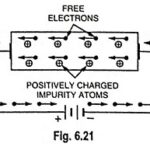
Continuity Equation in Semiconductor: The Continuity Equation in Semiconductor states a condition of dynamic equilibrium for the concentration of mobile carriers in any elementary volume of the semiconductor. In Fig. 6.21 we have seen that on disturbing the equilibrium concentrations of carriers … (Read More)
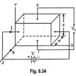
What is Hall Effect in Semiconductor?: When a specimen (metal or semiconductor) is placed in a transverse magnetic field and a direct current is passed through it, then an electric field is induced across its edges in the perpendicular direction of … (Read More)
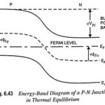
Basic Structure of PN Junction in Semiconductor: Most semiconductor devices employ one or more P-N junctions. The P-N junction is the control element for the performance of all semiconductor devices such as rectifiers, amplifiers, switching devices, linear and digital integrated circuits. … (Read More)
Equilibrium Conditions in Semiconductor Physics: The electron and hole concentrations, under thermal Equilibrium Conditions can be found by knowing the position of the Fermi energy EF with respect to the bottom of the conduction band energy EC and top of valence … (Read More)
Charge Neutrality Equation in Semiconductor: The semiconductor crystal is electrically neutral under thermal equilibrium conditions. The electrons are distributed among the different energy states, producing both negative and positive charges but the net charge density is zero. This charge neutrality condition … (Read More)
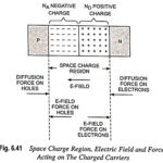
Space Charge Region at a Junction: As explained already, the interface separating the N and P-regions is called the metallurgical junction. Let us consider a step junction in which the doping concentration is uniform in each region but there is an … (Read More)
Zero bias PN junction: Here we will examine the properties of the step junction in thermal equilibrium, where no currents exist and no external excitation is applied. We will determine built-in potential barrier through the depletion … (Read More)
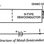
Metal Semiconductor Junctions: Metal semiconductor junctions are very common in all semiconductor devices and are very important. Depending upon the doping concentration, materials, and the characteristics of the interface, the metal semiconductor junctions can act as either an ohmic contact or … (Read More)
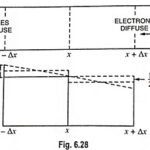
Explain Steady State Conditions in Semiconductor: When the P-N junction is forward biased, current flows quite freely P to N in a P-N junction, as discussed in Fig. 6.28. But when the P-N junction … (Read More)