Simple Diode Detector:
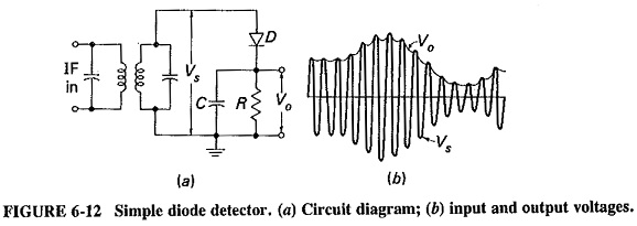
Operation of diode detector: The Simple Diode Detector is by far the most common device used for AM demodulation (or detection), and its operation will now be considered in detail. On the circuit of Figure 6-12a, C is a small capacitance and R is a large resistance. The parallel combination of R and C is the load resistance across which the rectified output voltage Vo is developed. At each positive peak of the RF cycle, C charges up to a potential almost equal to the peak signal voltage Vs.
The difference is due to the diode drop since the forward resistance of the diode is small (but not zero). Between peaks a little of the charge in C decays through R, to be replenished at the next positive peak. The result is the voltage Vo, which reproduces the modulating voltage accurately, except for the small amount of RF ripple. Note that the time constant of RC combination must be slow enough to keep the RF ripple as small as possible, but sufficiently fast for the Simple Diode Detector circuit to follow the fastest modulation variations.
This simple diode detector has the disadvantages that Vo, in addition to being proportional to the modulating voltage, also has a dc component, which represents the average envelope amplitude (i.e., carrier strength), and a small RF ripple. The unwanted components are removed in a practical detector, leaving only the intelligence and some second harmonic of the modulating signal.
Practical diode detector:
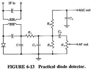
A number of additions have been made to the Simple Diode Detector, and its practical version is shown in Figure 6-13. The circuit operates in the following manner. The diode has been reversed, so that now the negative envelope is demodulated. This has no effect on detection, but it does ensure that a negative AGC voltage will be available, as will be shown. The resistor R of the basic circuit has been split into two parts (R1 and R2) to ensure that there is a series dc path to ground for the diode, but at the same time a low-pass filter has been added, in the form of R1 – C1. This has the function of removing any RF ripple that might still be present.
Capacitor C2 is a coupling capacitor, whose main function is to prevent the diode dc output from reaching the volume control R4. Although it is not necessary to have the volume control immediately after the detector, that is a convenient place for it. The combination R3 – C3 is a low-pass filter designed to remove AF components, providing a dc voltage whose amplitude is proportional to the carrier strength, and which may be used for automatic gain control.
It can be seen from Figure 6-13 that the dc diode load is equal to R1 + R2, whereas the audio load impedance Zm is equal to R1 in series with the parallel combination of R2, R3 and R4, assuming that the capacitors have reactances which may be ignored. This will be true at medium frequencies, but at high and low audio frequencies Zm may have a reactive component, causing a phase shift and distortion as well as an uneven frequency response.

