Small Signal Model of FET:
The Small Signal Model of FET which consists of Low Frequency Small Signal Model for FET and High Frequency Model for FET.
Low Frequency Model: In a FET, instantaneous drain current iD is a function of the instantaneous gate-source voltage vGS and instantaneous drain-source voltage vDS and is, therefore, expressed as
![]()
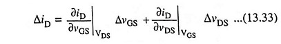
If both the gate and drain voltages are varied, the change in drain current is given approximately by the first two terms in the Taylor’s series expansion of Eq. (13.32) or
Using the conventional small signal notations, ΔiD, ΔvGS and ΔvDS may be replaced respectively by time varying components id, vgs and vds. Now Eq. (13.33) becomes
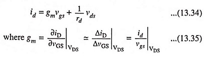
Parameter gm is the mutual conductance, or transconductance
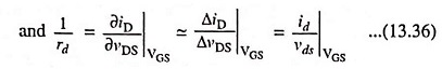
The reciprocal of rd is the drain conductance gd.
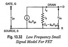
Circuit shown in Fig. 13.32 is made satisfying Eq. (13.34) giving the incremental drain current id in form of gm, rd, vgs and vds. This circuit forms the low frequency Small Signal Model of FET: This model consists of one dependent current generator whose current gmvgs is proportional to the time varying gate source voltage vgs and proportionality constant is the transconductance gm.
The arrow points from drain to source to indicate a phase change of 180° (or phase reversal) between output and input voltages as will occur in actual operation. In low frequency model, as the gate is reverse biased, the gate current becomes zero. So, in low frequency model, gate to source junction is represented by an open circuit and no current is drawn by the input terminal of the FET. The reason is that input resistance, (gate-to-source resistance) is very large. The output resistance is represented by the resistance rd (resistance from drain to source). If rd is sufficiently large as compared to those of other circuit elements, this is ignored. Now the equivalent circuit becomes simply a current source whose magnitude is controlled by vgs and gm—clearly a voltage controlled current source.
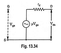
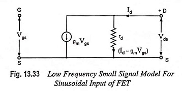
Small Signal Model of FET for sinusoidal input voltage of rms value Vgs may be drawn, as shown in Fig. 13.33 where vgs, id, vds have been replaced respectively by rms values Vgs, Id and Vds. The voltage-controlled current source (gm Vgs) can be replaced by equivalent voltage-controlled voltage source (μVgs) as depicted in Fig. 13.34.
Now the equivalent circuit consists of a voltage source (μVgs) in series with a drain resistance rd. Here μ is the amplification factor of the FET and is equal to the product of transconductance gm and drain resistance rd i.e., μ = gmrd.
Comparison of Low Frequency Models of FET and BJT:
- Both FET and BJT models have a dependent current generator in the output circuit.
- In FET models, the generator current is proportional to the input voltage Vgs while in BJT models, the generator current is proportional to the input current.
- In FET models input impedance is very high (theoretically infinite at low frequencies) while in common emitter BJT model the input impedance is of the order of 800 Ω.
- In FET, there is no feedback from output (drain) to the input (source) while in BJT models it is. Thus it can be safely said that at low frequencies, FET forms a more ideal amplifier than BJT amplifier.
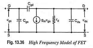
High Frequency Model: At low frequency, reactance offered by interelectrode capacitance is very large and, therefore, interelectrode capacitances do not appear in low frequency equivalent circuit. At higher frequencies device capacitances between terminals cause reduction in amplifier gain as capacitive impedance decreases with the increase in supply frequency. Such circuit capacitances resulted in due to device construction or stray wiring are shown as connected with dashed lines in the circuit of Fig. 13.35 to indicate that they are not capacitances that are connected into the circuit intentionally but arise as a result of the circuit and device construction.
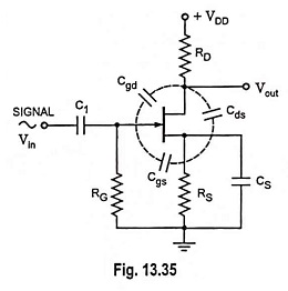
Figure 13.36 depicts the high frequency model of the FET which is identical with Fig. 13.32 except that the capacitances between the gate-source and gate-drain nodes are shown in the figure. The capacitor Cgs represents the barrier capacitance between gate and source, and Cgd is the barrier capacitance between gate and drain. The element Cds represents the drain to source capacitance of the channel. Because of these internal capacitances feedback exists between the input and output circuits of the FET and voltage amplification drops drastically with increase in frequency.