Step Up Converter or Boost Converter:
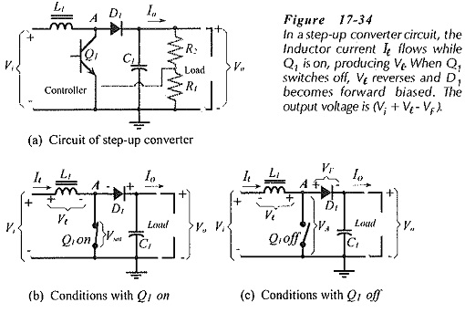
A Step Up Converter, or boost converter, produces a dc output voltage higher than its supply voltage. In the circuit shown in Fig. 17-34(a), L1 is directly connected to the supply, and D1 is in series with L1 and C1 The collector of Q1 is connected to the junction of L1 and D1 (point A), and its emitter is grounded.
When Q1 is on [Figure 17-34(b)], D1 is reverse biased, and
When Q1 is off [Figure 17-34(c)], Vl reverses polarity to keep Il flowing. The output voltage is now,
So, the output voltage is larger than the input, and its actual level can be set by selection of R1 and R2 [in Fig. 17-34(a)].
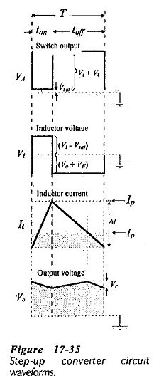
The voltage at point A has the pulse waveform (VA) illustrated in Fig. 17-35. During ton (Q1 on time), VA = Vsat, and during toff VA = (Vi + Vl). The inductor current increases to Ip during ton, and decreases during toff as L1 discharges to C1 and the load. The output voltage (Vo across C1) decreases during ton, because D1 is reverse biased and C1 is supplying all the load current. During toff D1 is forward biased and C1 is recharged from L1. Vo increases while Il is greater than Io, and decreases when Il is less than Io.
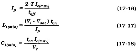
From the circuit conditions and the waveforms, the following equations can be derived:
Inverting Converter:
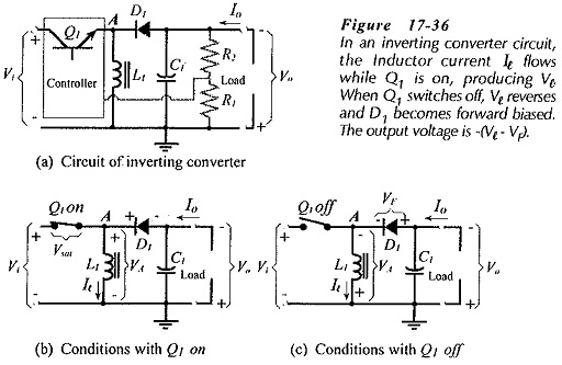
Figure 17-36(a) shows the circuit of an inverting converter, (also termed a flyback converter). This circuit produces a negative dc output voltage from a positive supply voltage. In this case, L1 is connected between ground and the emitter terminal of Q1, (point A). Diode D1 is in series with Q1 emitter and C1. Note the polarity of D1 and output capacitor C1.
Figure 17-36(b) shows that when Q1 is on, D1 is reverse biased, and
From Fig. 17-36(c), when Q1 is off Vl reverses to keep Il flowing. Diode D1 is now forward biased, giving
The output voltage is negative, and once again the actual output voltage level is set by selection of R1 and R2.
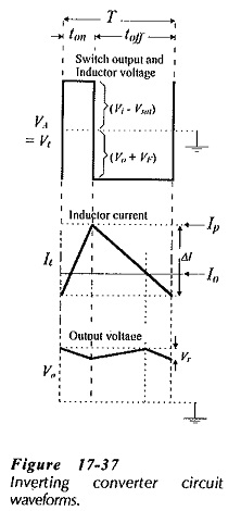
The voltage at point A in Fig. 17-36 is also the inductor voltage, and it has the pulse waveform shown in Fig. 17-37. During ton, VA = (Vi – Vsat); and during toff VA = -(Vo + VF). As in other switching converters, the inductor current increases to Ip during ton and decreases during toff, discharging to C1 and the load. Vo decreases during ton (D1 reverse biased) as C1 supplies all of Io. Then, C1 is recharged from L1 during toff (D1 forward biased), and Vo increases while Il exceeds Io, and decreases while Il is less than Io.
Equations 17-16, 17-17, and 17-18 apply for the inverting converter, as well as for the Step Up Converter.
