Transistor Buffer Circuit:
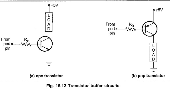
The Fig. 15.12 shows the Transistor Buffer Circuit. In these Transistor Buffer Circuit, transistor is used as a switch. It can be switch ON or OFF with logic 0 or logic 1 on port pin depending on the application. To make transistor ON with logic 0 at port pin we have to use pnp transistor otherwise we have to use npn transistor. When transistor is ON, its collector current drives the load. To determine component values and transistor we have check maximum collector current of the transistor (ICmax), maximum hfe that transistor can provide (hfemax), maximum collector to emitter breakdown voltage (VBCEO)and a maximum power dissipation (Pdmax) allowed by the transistor.
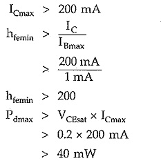
Let us assume that the load current is 200mA and maximum sourcing current of port pin is 1mA. Then Transistor Buffer Circuit should have
Assuming output high voltage of port pin equal to 4.5V we have
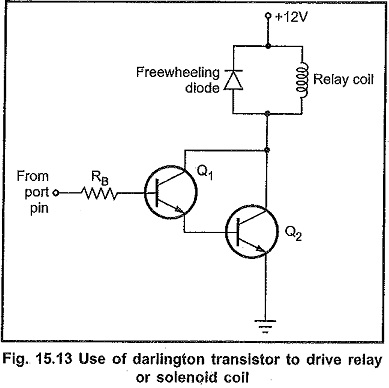
When load current requirements are more, one transistor is not sufficient to provide sufficient current gain. In such situations two transistors in darlington connection are used to provide the necessary current gain. The Fig. 15.13 shows the darling transistor pair used to drive relay or solenoid coil.
Here, the output port pin supplies the base current to transistor Q1. This base current produces β times large, collector current of Q1. The collector current of Q1 becomes the base current of Q2 and is amplified by the current gain of Q2, i.e. β2. Therefore, overall current amplification is β1 X β2. Usually this amplification is greater than 1000. Many such darlington pairs are available. We can use these Darlington pair to drive loads upto about 1A load currents.
As shown in the Fig. 15.13, free wheeling diode is purposely connected when load is inductive such as solenoid, relay and motor. We know that, inductor opposes change in current. When we switch off the transistor, the current in the inductor does not reach to zero immediately; it flows for a while. However, this current cannot flow through transistor, because it is off. Instead, this current develops a voltage across inductor with reverse polarities, i.e. – ve at the top and + ve at in the bottom in given circuit. Usually, this reverse voltage is large enough to break down the transistor. The free wheeling diode provides the path for induced current and clamps the reverse voltage across inductor at 0.7 V.
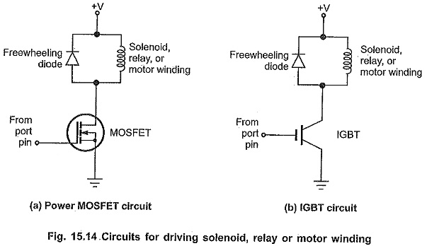
The Fig. 15.14 shows a power driver circuits using MOSFET and IGBT to drive solenoids, relay or motor windings. Power MOSFETS are somewhat more expensive than, darlington transistors, but they have the advantage that they require only a voltage to drive them. The IGBT has high input impedance and fast switching speed. They also have low voltage drop and high current carrying capacity.


