Types of Field Effect Transistor:
In general, Three Types of Field Effect Transistor are namely,
- Junction field effect transistor (JFET)
- Metal oxide semiconductor field effect transistor (MOSFET)
- Complementary Metal Oxide Semiconductor (CMOS)
Junction field effect transistor (JFET):
The basic processes used for the fabrication of JFET are exactly similar to those used in the fabrication of BJT.
The JFETs are further classified as
- N-channel JFET and
- P-channel JFET.
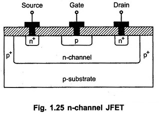
The development of n-channel JFET is as shown in the Fig. 1.25.
The JFET, the epitaxial layer is used as n-channel. The p+ gate is formed in n-type channel by ion-implantation or diffusion process. While good ohmic contacts are achieved by using n+ diffusion layers below drain and source regions.
Metal Oxide Semiconductor Field Effect Transistor (MOSFET):
Another Types of Field Effect Transistor is Metal oxide semiconductor field effect transistor (MOSFET). MOSFETs are classified as follows
- Enhancement mode MOSFET
- Depletion mode MOSFET
In MOSFETs gate terminal is isolated from the FET channel by silicon dioxide insulating layer. As the layer is insulating type, it provides very high input resistance. In providing superior barrier for impurities penetrating SiO2 layer, silicon nitride (Si3N4 ) is sandwitched between two silion dioxide (SiO2) layers. This helps in increasing overall dielectric constant.
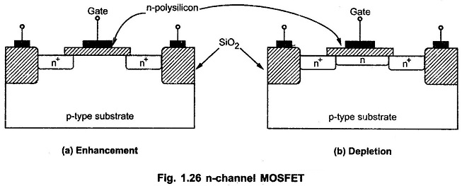
The n-channel MOSFET of enhancement and depletion mode are as shown in the Fig. 1.26 (a) and (b) respectively.
In the enhancement mode, MOSFET is in OFF state when gate-source bias is zero, while MOSFET turns ON by positive gate source voltage. in depletion mode, because of n-implanted channel conduction is possible in ON state for zero gate-source voltage. While negative gate source voltage is required to turn it OFF.
Complementary Metal Oxide Semiconductor (CMOS):
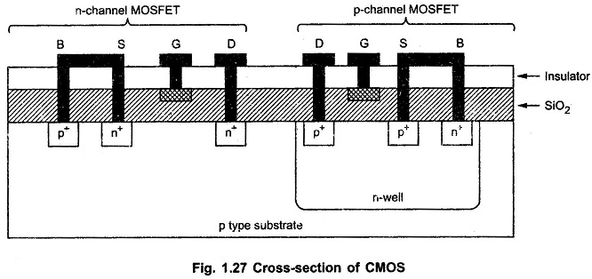
When n-channel MOSFET and p-channel MOSFET both are integrated on same chip, the device is termed as complementary CMOS. In this Types of Field Effect Transistor CMOS fabrication, n-type well is diffused in p-type substrate. Also p-channel MOSFET is fabricated within this n-well. Basically this n-well forms substrate for p-channel MOSFET.
In the fabrication of p-channel MOSFET two additional steps are required as compared to n-channel MOSFET fabrication. The additional steps are formation of n-well and ion-implantation of p-type source and drain regions. The cross section of CMOS IC is as shown in the Fig. 1.27.


