Voltage Variable Capacitors:
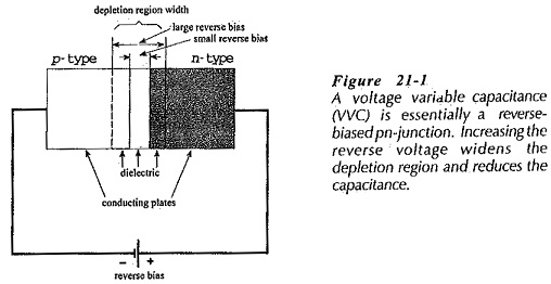
VVC Operation – Voltage Variable Capacitors diodes (VVCs) are also known as varicaps, varactors, and as tuning diodes. Basically, a Voltage Variable Capacitors is a reverse biased diode, and its capacitance is the junction capacitance. Recall that the width of the depletion region at a pn-junction depends upon the reverse bias voltage, (Fig. 21-1). A large reverse bias produces a wide depletion region, and a small reverse bias gives a narrow depletion region. The depletion region acts as a dielectric between two conducting plates, so the junction behaves as a capacitor.
The depletion layer capacitance (Cpn) is proportional to the junction area and inversely proportional to the width of the depletion region. Because the depletion region width is proportional to the reverse bias voltage, Cpn is inversely proportional to the reverse bias voltage. This is not a direct proportionality; instead Cpn is proportional to 1/Vn, where V is the reverse bias voltage, and n depends upon doping density.
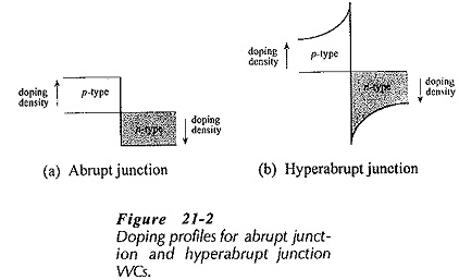
Figure 21-2 shows the doping profiles for two types of Voltage Variable Capacitors classified as abrupt junction and hyperabrupt junction devices. In the abrupt junction WC. the semiconductor material is uniformly doped, and it changes abruptly from p-type to n-type at the junction. The hyperabrupt junction device has the doping density increased close to the junction. This increasing density produces a narrower depletion region, and so it results in a larger junction capacitance. It also causes the depletion region width to be more sensitive to bias voltage variations, thus it produces the largest capacitance change for a given voltage variation. VVCs are packaged just like ordinary low-current diodes.
Equivalent Circuit:
The complete equivalent circuit for a Voltage Variable Capacitors is shown in Fig. 21-3(a), and a simplified version is given in Fig. 21-3(b). In the complete circuit, the junction capacitance (CJ) is shunted by the junction reverse leakage resistance (RJ). The resistance of the semiconductor material is represented by RS, the terminal inductance is LS, and the capacitance of the terminals (or the device package) is CC. Because LS is normally very small and RJ is very large, the equivalent circuit can be simplified [Fig 21-3(b)] to RS in series with CT, where CT is the sum of the junction and terminal capacitances, (CT = CJ + CC). The Q-factor for a VVC can be as high as 600 at a 50 MHz frequency. However, Q-factor varies with bias voltage and frequency, so it is used only as a figure of merit for comparing the performance of different VVCs.
Specification and Characteristics:
A wide selection of nominal WC capacitances is available, ranging approximately from 6 pF to 700 pF. The capacitance tuning ratio (TR) is the ratio of CT at a small reverse voltage to CT at a large reverse voltage. In the partial specification for a VVC shown in Fig. 21-4, the tuning ratio is listed as C1/C10. This is the ratio of the device capacitance at 1 V reverse bias to that at a 10 V reverse bias. Using the 400 pF minimum capacitance (CT) listed for a 1 V bias, the capacitance is changed to 400 pF/ 14 when the bias is 10 V. The specification also lists the Q-factor, as well as maximum reverse voltage, reverse leakage current, and the maximum forward current that can be passed when the device is forward biased.
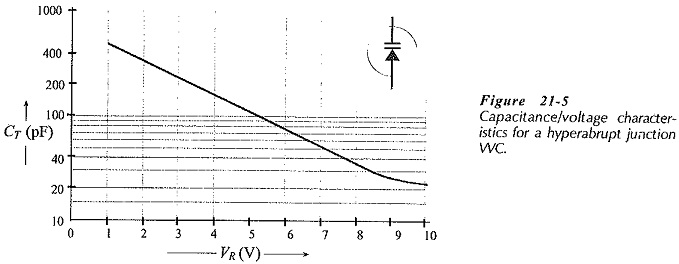
A typical graph of capacitance (CT) versus reverse bias voltage (VR) for a hyperabrupt junction VVC is reproduced in Fig. 21-5 together with the VVC circuit symbol. It is seen that CT varies (approximately) from 500 pF to 25 pF when VR is changed from 1 V to 10 V. It should be noted from the specification in Fig. 21-4 that the nominal capacitance has a large tolerance (400 pF to 600 pF), and this must be taken into account when using the CT/ VR graphs.
Applications:
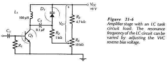
The major application of Voltage Variable Capacitors is as tuning capacitors to adjust the frequency of resonance circuits. An example of this is the circuit shown in Fig. 21-6, which is an amplifier with a tuned circuit load. The amplifier produces an output at the resonance frequency of the tuned circuit. The VVC provides the capacitance (CT) of the resonant circuit, and this can be altered by adjusting the diode (reverse) bias voltage (VD). So, the resonance frequency of the circuit can be varied. C1 is a coupling capacitor with a capacitance much larger than that of the VVC, and R2 limits the VVC forward current in the event that it becomes forward biased.


